 |
Electronic Components Datasheet Search |
|
|
Electronic Components Datasheet Search |
|
The question interval is too short.
Please try again in a few seconds.

Hello, Please ask a question about OP77 Datasheet
# Example questions:
➢ Compare the typical input bias current at 25°c versus its variation over a temperature range of -75°c to 125°c, based on figure 13 and figure 14. what does this suggest about the circuit's stability over a wide temperature range?
➢ Referring to figures 4, 5, and 6, what is the approximate range of open-loop gain variation over temperature and offset voltage variations? what could be done to mitigate these variations in a precision application?
➢ Analyze figure 9. how does the closed-loop response change with different gain configurations? what implications does this have for the overall system design and required bandwidth?
| Part No. | OP77 |
| Manufacturer | AD |
| Size | 380 Kbytes |
| Pages | 16 pages |
| Description | Next Generation OP07 Ultralow Offset Voltage Operational Amplifier |






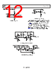



1. General Description & Key Features
️· Precision Operational Amplifier: The OP77 is described as a high-precision, low-noise operational amplifier.
️· Key Benefits: It's designed for applications requiring very accurate amplification and signal processing.
2. Absolute Maximum Ratings
️· Supply Voltage (±Vs): ±18V
️· Common-Mode Voltage: 18V
️· Input Voltage (Differential): ±0.5V
️· Power Dissipation: 400mW (depending on package and mounting)
️· Operating Temperature Range: -55°C to +125°C
️· Storage Temperature Range: -65°C to +150°C
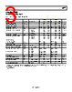
3. Electrical Characteristics (Typical at T = 25°C unless otherwise noted)
️· Input Offset Voltage: Typically 2.5 mV (Maximum 7 mV)
️· Input Bias Current: Typically 1 pA (Maximum 4 pA)
️· Input Offset Current: Typically 1 pA (Maximum 4 pA)
️· Open-Loop Gain: Typically 100 dB (Vout/Vin at 1kHz)
️· Supply Current: Less than 2 mA
️· Slew Rate: 0.4 V/µs
️· Unity Gain Bandwidth: 1.1 MHz
️· Common-Mode Rejection Ratio (CMRR): 100 dB
️· Power Supply Rejection Ratio (PSRR): 100 dB
️· Noise Voltage: 8 nV/√Hz at 1kHz
️· Thermal Offset: 20 µV/°C (max)
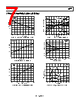
4. Graphs & Figures (Brief Summary – Important for application understanding)
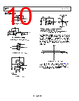
️· Figures 2-15: These graphs provide critical application data:
- Gain/Phase Response (Fig. 2): Shows the open-loop gain and phase shift across frequency. Important for stability in feedback configurations.
- CMRR vs. Frequency (Fig. 11): High CMRR across a wide frequency range.
- PSRR vs. Frequency (Fig. 12): High PSRR across a wide frequency range.
- Input Offset Voltage vs. Temperature (Fig. 14): Shows the relationship between input offset voltage and temperature, important for temperature-sensitive applications.
- Input Bias/Offset Current vs. Temperature (Fig. 14): Shows how these currents change with temperature.
- Open-Loop Gain vs. Temperature (Fig. 1): How the gain changes with temperature.
- Warm-Up Drift (Fig. 7): Shows how the offset voltage changes over time after power-up.
- Offset Voltage Change Due to Thermal Shock (Fig. 15): Describes the change in offset voltage due to a sudden temperature change.
5. Applications (Implied)
Based on the datasheet's descriptions and characteristics, the OP77 is suitable for:
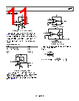
️· Instrumentation Amplifiers: Its low offset voltage and current make it ideal for precise measurements.
️· Precision Filter Circuits: The clean signal and low noise are essential for accurate filtering.
️· High-Accuracy Signal Conditioning: Amplifying and processing signals where minimal error is critical.
️· Data Acquisition Systems: Ensuring the integrity of analog signals before digitization.
1. General Description & Key Features
️· Precision Operational Amplifier: The OP77 is described as a high-precision, low-noise operational amplifier.
️· Key Benefits: It's designed for applications requiring very accurate amplification and signal processing.
2. Absolute Maximum Ratings
️· Supply Voltage (±Vs): ±18V
️· Common-Mode Voltage: 18V
️· Input Voltage (Differential): ±0.5V
️· Power Dissipation: 400mW (depending on package and mounting)
️· Operating Temperature Range: -55°C to +125°C
️· Storage Temperature Range: -65°C to +150°C
3. Electrical Characteristics (Typical at T = 25°C unless otherwise noted)
️· Input Offset Voltage: Typically 2.5 mV (Maximum 7 mV)
️· Input Bias Current: Typically 1 pA (Maximum 4 pA)
️· Input Offset Current: Typically 1 pA (Maximum 4 pA)
️· Open-Loop Gain: Typically 100 dB (Vout/Vin at 1kHz)
️· Supply Current: Less than 2 mA
️· Slew Rate: 0.4 V/µs
️· Unity Gain Bandwidth: 1.1 MHz
️· Common-Mode Rejection Ratio (CMRR): 100 dB
️· Power Supply Rejection Ratio (PSRR): 100 dB
️· Noise Voltage: 8 nV/√Hz at 1kHz
️· Thermal Offset: 20 µV/°C (max)
4. Graphs & Figures (Brief Summary – Important for application understanding)
️· Figures 2-15: These graphs provide critical application data:
- Gain/Phase Response (Fig. 2): Shows the open-loop gain and phase shift across frequency. Important for stability in feedback configurations.
- CMRR vs. Frequency (Fig. 11): High CMRR across a wide frequency range.
- PSRR vs. Frequency (Fig. 12): High PSRR across a wide frequency range.
- Input Offset Voltage vs. Temperature (Fig. 14): Shows the relationship between input offset voltage and temperature, important for temperature-sensitive applications.
- Input Bias/Offset Current vs. Temperature (Fig. 14): Shows how these currents change with temperature.
- Open-Loop Gain vs. Temperature (Fig. 1): How the gain changes with temperature.
- Warm-Up Drift (Fig. 7): Shows how the offset voltage changes over time after power-up.
- Offset Voltage Change Due to Thermal Shock (Fig. 15): Describes the change in offset voltage due to a sudden temperature change.
5. Applications (Implied)
Based on the datasheet's descriptions and characteristics, the OP77 is suitable for:
️· Instrumentation Amplifiers: Its low offset voltage and current make it ideal for precise measurements.
️· Precision Filter Circuits: The clean signal and low noise are essential for accurate filtering.
️· High-Accuracy Signal Conditioning: Amplifying and processing signals where minimal error is critical.
️· Data Acquisition Systems: Ensuring the integrity of analog signals before digitization.
| Part No. | OP77 |
| Manufacturer | AD |
| Size | 380 Kbytes |
| Pages | 16 pages |
| Description | Next Generation OP07 Ultralow Offset Voltage Operational Amplifier |
| Does ALLDATASHEET help your business so far? [ DONATE ] |
About Alldatasheet | Advertisement | Contact us | Privacy Policy | Link to Datasheet | Link Exchange | Manufacturer List All Rights Reserved©Alldatasheet.com |
| Russian : Alldatasheetru.com | Korean : Alldatasheet.co.kr | Spanish : Alldatasheet.es | French : Alldatasheet.fr | Italian : Alldatasheetit.com Portuguese : Alldatasheetpt.com | Polish : Alldatasheet.pl | Vietnamese : Alldatasheet.vn Indian : Alldatasheet.in | Mexican : Alldatasheet.com.mx | British : Alldatasheet.co.uk | New Zealand : Alldatasheet.co.nz |
|
Family Site : ic2ic.com |
icmetro.com |
 Indian ▼
  English
 Chinese
 German
 Japanese
 Russian
 Korean
 Spanish
 French
 Italian
 Portuguese
 Polish
 Vietnamese
 Mexican
 British
 New Zealand