 |
Electronic Components Datasheet Search |
|
|
Electronic Components Datasheet Search |
|
The question interval is too short.
Please try again in a few seconds.

Hello, Please ask a question about AP2301EN-HF_14 Datasheet
# Example questions:
➢ What is the typical on-state resistance (rds(on)) of the ap2301en at a junction temperature of 25°c and what factor influences its variation?
➢ What does the 'effective transient thermal impedance' represent, and why is it important for pulsed load applications?
➢ What is the maximum safe operating area of the ap2301en, and what parameters define its boundaries?
| Part No. | AP2301EN-HF_14 |
| Manufacturer | A-POWER |
| Size | 102 Kbytes |
| Pages | 4 pages |
| Description | Small Package Outline |


1. General Information / Features:
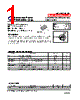
️· Device Type: N-Channel MOSFET
️· Voltage Rating (VDS): 30V
️· Drain Current (ID): 4.2 A (Continuous)
️· Power Dissipation (PD): 12W
️· Logic Level Gate Drive: Implies suitability for low-voltage logic circuits.
️· Small Size: Likely intended for compact circuit designs.
2. Electrical Characteristics (Key Parameters):
️· VDS (Drain-Source Voltage): 30V (Maximum)
️· ID (Drain Current): 4.2 A (Continuous at case temperature of 70°C). This is a crucial rating to avoid overheating.
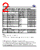
️· RDS(on) (Drain-Source On-Resistance): 0.053 Ohms @ VGS = 4.5V, ID = 2.1A (This is a key indicator of efficiency - lower RDS(on) means less power loss).
️· VGS(th) (Gate-Source Threshold Voltage): 1.0V (Max) - Defines the voltage required to turn the MOSFET 'on'.
️· Input Capacitance (Ciss): 37.6 pF (Influences switching speed)
️· Output Capacitance (Coss): 9.8 pF (Important for high-frequency operation)
️· Gate Charge (Qg): 6.2 nC (Affects switching speed and driver requirements)
3. Thermal Characteristics:
️· TJ(max) (Maximum Junction Temperature): 150°C (Critical to avoid permanent damage).
️· RθJC (Thermal Resistance, Junction-to-Case): 35°C/W (Important for thermal management and heat sinking). A lower value is better.
️· RθJA (Thermal Resistance, Junction-to-Ambient): Implies a value based on the mounting condition (not explicitly given in the text but is a calculated parameter).
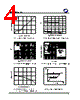
️· Safe Operating Area (SOA) Graph (Fig. 9): Shows the limits of continuous drain current versus ambient temperature.
️· Effective Transient Thermal Impedance (Fig. 10): Shows how quickly the junction temperature rises during pulsed operation, critical for pulsed power applications.
4. Switching Characteristics and Waveforms:
️· Gate Charge Waveform (Fig. 12): Illustrates the charge distribution during switching.
️· Typical Capacitance Characteristics: Shows capacitance values at different voltage levels.
5. Graphs and Figures (Illustrating Key Behaviors):
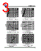
️· On-Resistance vs. Gate Voltage (Fig. 3): Shows how RDS(on) changes with VGS.
️· Normalized On-Resistance vs. Junction Temperature (Fig. 4): Demonstrates the impact of temperature on RDS(on).
️· Forward Characteristic of Reverse Diode (Fig. 5): Shows the reverse diode characteristics.
️· Gate Threshold Voltage vs. Junction Temperature (Fig. 6): Shows how VGS(th) changes with temperature.
️· Maximum Continuous Drain Current vs. Ambient Temperature (Fig. 11): Important for thermal design.
6. Notes/Cautions/Important Considerations:
️· Power Dissipation Limits: Carefully manage power dissipation to stay within the specified limits (12W) to avoid overheating.
️· Thermal Management: Consider heat sinking or other thermal management techniques if operating at high currents or in high-temperature environments.
️· Safe Operating Area (SOA): Operate within the limits defined by the SOA graph to prevent device failure.
️· Gate Drive Voltage: Ensure the gate drive voltage is appropriate for the MOSFET's characteristics.
️· RDS(on) and Efficiency: Pay attention to RDS(on) to minimize power losses and improve efficiency.
1. General Information / Features:
️· Device Type: N-Channel MOSFET
️· Voltage Rating (VDS): 30V
️· Drain Current (ID): 4.2 A (Continuous)
️· Power Dissipation (PD): 12W
️· Logic Level Gate Drive: Implies suitability for low-voltage logic circuits.
️· Small Size: Likely intended for compact circuit designs.
2. Electrical Characteristics (Key Parameters):
️· VDS (Drain-Source Voltage): 30V (Maximum)
️· ID (Drain Current): 4.2 A (Continuous at case temperature of 70°C). This is a crucial rating to avoid overheating.
️· RDS(on) (Drain-Source On-Resistance): 0.053 Ohms @ VGS = 4.5V, ID = 2.1A (This is a key indicator of efficiency - lower RDS(on) means less power loss).
️· VGS(th) (Gate-Source Threshold Voltage): 1.0V (Max) - Defines the voltage required to turn the MOSFET 'on'.
️· Input Capacitance (Ciss): 37.6 pF (Influences switching speed)
️· Output Capacitance (Coss): 9.8 pF (Important for high-frequency operation)
️· Gate Charge (Qg): 6.2 nC (Affects switching speed and driver requirements)
3. Thermal Characteristics:
️· TJ(max) (Maximum Junction Temperature): 150°C (Critical to avoid permanent damage).
️· RθJC (Thermal Resistance, Junction-to-Case): 35°C/W (Important for thermal management and heat sinking). A lower value is better.
️· RθJA (Thermal Resistance, Junction-to-Ambient): Implies a value based on the mounting condition (not explicitly given in the text but is a calculated parameter).
️· Safe Operating Area (SOA) Graph (Fig. 9): Shows the limits of continuous drain current versus ambient temperature.
️· Effective Transient Thermal Impedance (Fig. 10): Shows how quickly the junction temperature rises during pulsed operation, critical for pulsed power applications.
4. Switching Characteristics and Waveforms:
️· Gate Charge Waveform (Fig. 12): Illustrates the charge distribution during switching.
️· Typical Capacitance Characteristics: Shows capacitance values at different voltage levels.
5. Graphs and Figures (Illustrating Key Behaviors):
️· On-Resistance vs. Gate Voltage (Fig. 3): Shows how RDS(on) changes with VGS.
️· Normalized On-Resistance vs. Junction Temperature (Fig. 4): Demonstrates the impact of temperature on RDS(on).
️· Forward Characteristic of Reverse Diode (Fig. 5): Shows the reverse diode characteristics.
️· Gate Threshold Voltage vs. Junction Temperature (Fig. 6): Shows how VGS(th) changes with temperature.
️· Maximum Continuous Drain Current vs. Ambient Temperature (Fig. 11): Important for thermal design.
6. Notes/Cautions/Important Considerations:
️· Power Dissipation Limits: Carefully manage power dissipation to stay within the specified limits (12W) to avoid overheating.
️· Thermal Management: Consider heat sinking or other thermal management techniques if operating at high currents or in high-temperature environments.
️· Safe Operating Area (SOA): Operate within the limits defined by the SOA graph to prevent device failure.
️· Gate Drive Voltage: Ensure the gate drive voltage is appropriate for the MOSFET's characteristics.
️· RDS(on) and Efficiency: Pay attention to RDS(on) to minimize power losses and improve efficiency.
| Part No. | AP2301EN-HF_14 |
| Manufacturer | A-POWER |
| Size | 102 Kbytes |
| Pages | 4 pages |
| Description | Small Package Outline |
| Does ALLDATASHEET help your business so far? [ DONATE ] |
About Alldatasheet | Advertisement | Contact us | Privacy Policy | Link to Datasheet | Link Exchange | Manufacturer List All Rights Reserved©Alldatasheet.com |
| Russian : Alldatasheetru.com | Korean : Alldatasheet.co.kr | Spanish : Alldatasheet.es | French : Alldatasheet.fr | Italian : Alldatasheetit.com Portuguese : Alldatasheetpt.com | Polish : Alldatasheet.pl | Vietnamese : Alldatasheet.vn Indian : Alldatasheet.in | Mexican : Alldatasheet.com.mx | British : Alldatasheet.co.uk | New Zealand : Alldatasheet.co.nz |
|
Family Site : ic2ic.com |
icmetro.com |
 Indian ▼
  English
 Chinese
 German
 Japanese
 Russian
 Korean
 Spanish
 French
 Italian
 Portuguese
 Polish
 Vietnamese
 Mexican
 British
 New Zealand