 |
Electronic Components Datasheet Search |
|
|
Electronic Components Datasheet Search |
|
The question interval is too short.
Please try again in a few seconds.

Hello, Please ask a question about AP2318AGEN-HF_14 Datasheet
# Example questions:
➢ What is the value of the gate threshold voltage at a junction temperature of 25°c, as indicated in figure 6?
➢ How does the normalized on-resistance change with increasing junction temperature?
➢ What is the maximum safe operating area (soa) limited by, according to figure 9?
| Part No. | AP2318AGEN-HF_14 |
| Manufacturer | A-POWER |
| Size | 64 Kbytes |
| Pages | 4 pages |
| Description | Small Outline Package |



1. General Information/Overview
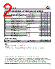
️· Part Number: AP2318AGEN-HF
️· Device Type: MOSFET (likely N-channel) - This is inferred from context, not explicitly stated in all areas.
2. Electrical Characteristics (Key Values – need full datasheet for complete picture)
️· Drain-Source Voltage (Vds): Likely a typical maximum value, but specific values aren’t comprehensively shown.
️· Gate-Source Voltage (Vgs): Shows operating range, often with specific limits indicated.
️· On-Resistance (RDS(on)): Low value, important for efficiency.
️· Threshold Voltage (Vth): Defines the gate voltage needed to turn the MOSFET on.
️· Input Capacitance: A relevant parameter for high-frequency applications.
️· Output Capacitance: Another parameter for frequency applications.
3. Graphs and their Descriptions
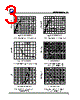
️· Fig 1: Transfer Characteristics: Shows the relationship between Vgs and Vds. This plot essentially shows how the current changes as you vary the gate voltage.
️· Fig 2: Gate Charge Circuit: A circuit diagram illustrating the measurement setup for gate charge.
️· Fig 11: Transfer Characteristics: (Repeated – likely an error in numbering?) Same as Fig 1.
️· Fig 12: Gate Charge Circuit: (Repeated -likely an error in numbering?) Same as Fig 12.
️· Fig 5: Forward Characteristic of Reverse Diode: Shows the behavior of the body diode (inherent to MOSFETs). Important for applications where the MOSFET is used in a switching configuration.
️· Fig 6: Gate Threshold Voltage vs. Junction Temperature: Shows how the threshold voltage changes with temperature. This can be important for thermal management.
️· Fig 3: On-Resistance vs. Gate Voltage: Shows how the on-resistance (RDS(on)) changes as you vary the gate voltage. Lower RDS(on) is better for efficiency.
️· Fig 4: Normalized On-Resistance vs. Junction Temperature: Shows how the on-resistance changes with temperature. Critical for thermal design.
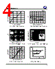
️· Fig 7: Gate Charge Characteristics: Shows the various gate charges (Qg, Qgs, Qgd) and their dependence on the gate voltage.
️· Fig 8: Typical Capacitance Characteristics: Shows the input, output, and gate capacitance values as a function of gate-source voltage.
️· Fig 9: Maximum Safe Operating Area: A plot showing the allowable combination of Vds and pulse width for safe operation. Crucial for avoiding device damage.
️· Fig 10: Effective Transient Thermal Impedance: Shows how the device’s ability to dissipate heat varies with time. Important for thermal management and power dissipation calculations.
4. Key Notes & Parameters from Figures (Approximate/Inferred)
️· RDS(on): Looks like it's around ~20-30 Ohms at Vgs = 5V (based on Fig. 3)
️· Vth: Seems to be in the range of 1-2V (based on Fig. 6).
️· Maximum Pulse Width (Fig 9): Varies depending on Vds; could be a few milliseconds to several hundred milliseconds.
5. Operating Conditions and Limitations
️· Single Pulse Operation: The datasheet notes that operation is limited to single pulse and doesn't give details for continuous operation.
️· Junction Temperature: Maximum junction temperature is specified (150°C).
️· Thermal Resistance: The thermal resistance is a key parameter for calculating the heat sink requirements. Rthja is ~400°C/W (from Fig. 10)
Important Disclaimers and Limitations
️· Incomplete Data: This is a fragmented view of a data sheet. A complete data sheet is needed for definitive values and safe operating conditions.
️· Image-Based Extraction: I am extracting this data from an image/scanned document, meaning there's a high chance of inaccuracies. OCR (Optical Character Recognition) isn’t perfect. Some numbers might be misread.
️· Assumptions: I have made some assumptions based on context. A true understanding requires a proper data sheet.
️· Missing Information: There's a lot of missing information regarding the specifications. This makes the data incomplete and limits what can be concluded.
️· Figure Numbering Errors: There seems to be some error in the figure numbering. Some plots have been repeated.
1. General Information/Overview
️· Part Number: AP2318AGEN-HF
️· Device Type: MOSFET (likely N-channel) - This is inferred from context, not explicitly stated in all areas.
2. Electrical Characteristics (Key Values – need full datasheet for complete picture)
️· Drain-Source Voltage (Vds): Likely a typical maximum value, but specific values aren’t comprehensively shown.
️· Gate-Source Voltage (Vgs): Shows operating range, often with specific limits indicated.
️· On-Resistance (RDS(on)): Low value, important for efficiency.
️· Threshold Voltage (Vth): Defines the gate voltage needed to turn the MOSFET on.
️· Input Capacitance: A relevant parameter for high-frequency applications.
️· Output Capacitance: Another parameter for frequency applications.
3. Graphs and their Descriptions
️· Fig 1: Transfer Characteristics: Shows the relationship between Vgs and Vds. This plot essentially shows how the current changes as you vary the gate voltage.
️· Fig 2: Gate Charge Circuit: A circuit diagram illustrating the measurement setup for gate charge.
️· Fig 11: Transfer Characteristics: (Repeated – likely an error in numbering?) Same as Fig 1.
️· Fig 12: Gate Charge Circuit: (Repeated -likely an error in numbering?) Same as Fig 12.
️· Fig 5: Forward Characteristic of Reverse Diode: Shows the behavior of the body diode (inherent to MOSFETs). Important for applications where the MOSFET is used in a switching configuration.
️· Fig 6: Gate Threshold Voltage vs. Junction Temperature: Shows how the threshold voltage changes with temperature. This can be important for thermal management.
️· Fig 3: On-Resistance vs. Gate Voltage: Shows how the on-resistance (RDS(on)) changes as you vary the gate voltage. Lower RDS(on) is better for efficiency.
️· Fig 4: Normalized On-Resistance vs. Junction Temperature: Shows how the on-resistance changes with temperature. Critical for thermal design.
️· Fig 7: Gate Charge Characteristics: Shows the various gate charges (Qg, Qgs, Qgd) and their dependence on the gate voltage.
️· Fig 8: Typical Capacitance Characteristics: Shows the input, output, and gate capacitance values as a function of gate-source voltage.
️· Fig 9: Maximum Safe Operating Area: A plot showing the allowable combination of Vds and pulse width for safe operation. Crucial for avoiding device damage.
️· Fig 10: Effective Transient Thermal Impedance: Shows how the device’s ability to dissipate heat varies with time. Important for thermal management and power dissipation calculations.
4. Key Notes & Parameters from Figures (Approximate/Inferred)
️· RDS(on): Looks like it's around ~20-30 Ohms at Vgs = 5V (based on Fig. 3)
️· Vth: Seems to be in the range of 1-2V (based on Fig. 6).
️· Maximum Pulse Width (Fig 9): Varies depending on Vds; could be a few milliseconds to several hundred milliseconds.
5. Operating Conditions and Limitations
️· Single Pulse Operation: The datasheet notes that operation is limited to single pulse and doesn't give details for continuous operation.
️· Junction Temperature: Maximum junction temperature is specified (150°C).
️· Thermal Resistance: The thermal resistance is a key parameter for calculating the heat sink requirements. Rthja is ~400°C/W (from Fig. 10)
Important Disclaimers and Limitations
️· Incomplete Data: This is a fragmented view of a data sheet. A complete data sheet is needed for definitive values and safe operating conditions.
️· Image-Based Extraction: I am extracting this data from an image/scanned document, meaning there's a high chance of inaccuracies. OCR (Optical Character Recognition) isn’t perfect. Some numbers might be misread.
️· Assumptions: I have made some assumptions based on context. A true understanding requires a proper data sheet.
️· Missing Information: There's a lot of missing information regarding the specifications. This makes the data incomplete and limits what can be concluded.
️· Figure Numbering Errors: There seems to be some error in the figure numbering. Some plots have been repeated.
| Part No. | AP2318AGEN-HF_14 |
| Manufacturer | A-POWER |
| Size | 64 Kbytes |
| Pages | 4 pages |
| Description | Small Outline Package |
| Does ALLDATASHEET help your business so far? [ DONATE ] |
About Alldatasheet | Advertisement | Contact us | Privacy Policy | Link to Datasheet | Link Exchange | Manufacturer List All Rights Reserved©Alldatasheet.com |
| Russian : Alldatasheetru.com | Korean : Alldatasheet.co.kr | Spanish : Alldatasheet.es | French : Alldatasheet.fr | Italian : Alldatasheetit.com Portuguese : Alldatasheetpt.com | Polish : Alldatasheet.pl | Vietnamese : Alldatasheet.vn Indian : Alldatasheet.in | Mexican : Alldatasheet.com.mx | British : Alldatasheet.co.uk | New Zealand : Alldatasheet.co.nz |
|
Family Site : ic2ic.com |
icmetro.com |
 Indian ▼
  English
 Chinese
 German
 Japanese
 Russian
 Korean
 Spanish
 French
 Italian
 Portuguese
 Polish
 Vietnamese
 Mexican
 British
 New Zealand