 |
Electronic Components Datasheet Search |
|
|
Electronic Components Datasheet Search |
|
The question interval is too short.
Please try again in a few seconds.

Hello, Please ask a question about AP2323AGN-HF_14 Datasheet
# Example questions:
➢ How does the gate threshold voltage (vgs(th)) change as the junction temperature increases from 25°c to 150°c?
➢ What is the typical value of rds(on) at a vgs of 10v and a drain current of 4a, according to the datasheet?
➢ What is the maximum allowable pulse width for a drain current of 20a?
| Part No. | AP2323AGN-HF_14 |
| Manufacturer | A-POWER |
| Size | 104 Kbytes |
| Pages | 4 pages |
| Description | Small Package Outline |

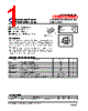
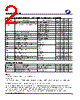
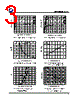
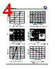

1. Device Overview
️· Product: AP2323AGN HF
️· Type: Power MOSFET (likely N-Channel, although not explicitly stated - assumption based on typical power MOSFET operation)
️· Function: High-performance switching application.
2. Absolute Maximum Ratings (Not Explicitly Listed, but implied by figures and text)
️· VDS (Drain-Source Voltage): Likely >30V (implied by figures and typical MOSFET ratings)
️· ID (Drain Current): Likely >25A (implied by graphs)
️· Tj (Junction Temperature): Figure 12 shows this can get quite high, likely up to 150°C but with derating.
️· Ta (Ambient Temperature): Figure 12 shows this can go up to 125°C.
️· PD (Power Dissipation): Likely limited by thermal characteristics (see Safe Operating Area graph, Figure 9).
3. Electrical Characteristics (Key Values)
️· RDS(on) (Drain-Source On-Resistance): This is a key parameter for efficiency. It's not given a simple value, but is discussed in relation to temperature (see figure 11), suggesting it’s relatively low. Figure 11 is very critical to understanding its behavior.
️· VGS(th) (Gate-Source Threshold Voltage): Not directly specified, but figures suggest a relatively low value, likely around 1-2V. Figure 2 shows the relationship to junction temperature.
️· Input Capacitance (Ciss): Figure 7 presents this as a function of drain-source voltage.
️· Output Capacitance (Coss): Figure 7 presents this as a function of drain-source voltage.
️· Gate Charge (Qg): Figure 7 shows this is a function of gate voltage.
4. Thermal Characteristics
️· Rthja (Junction-to-Ambient Thermal Resistance): This is crucial for determining how hot the device will get in a given application. Figure 10 presents this as a function of ambient temperature. The value is highly dependent on the thermal design of the printed circuit board (PCB) and heat sink used. It's stated that Rthja = 270°C/W.
️· Safe Operating Area (SOA): Figure 9 demonstrates the allowable combination of drain voltage and drain current, limited by power dissipation and junction temperature. It's critical *not* to exceed the limits shown on this graph.
5. Key Figures and Their Significance
️· Figure 8 (Drain Current vs. Ambient Temperature): Shows how the drain current varies with the ambient temperature.
️· Figure 11 (Transfer Characteristics): Describes the relationship between gate-source voltage (VGS) and drain-source voltage (VDS).
️· Figure 12 (Drain Current vs. Junction Temperature): Demonstrates the relationship between drain current and junction temperature.
️· Figure 9 (Safe Operating Area): Defines the safe operating limits for the device, based on voltage and current.
️· Figure 10 (Thermal Resistance): Shows the impact of ambient temperature on the MOSFET’s ability to dissipate heat.
️· Figure 7 (Capacitance Characteristics): Presents the input and output capacitances as a function of voltage.
️· Figure 2 (Threshold Voltage vs. Temperature): Shows how the threshold voltage changes with temperature.
6. Considerations for Use
️· Thermal Management is Critical: The MOSFET generates heat, so proper heat sinking and PCB layout are *essential* to prevent overheating and damage.
️· Safe Operating Area: Carefully check the combination of voltage and current to ensure operation within the SOA limits.
️· Gate Driving: Appropriate gate drive circuitry is needed to control the MOSFET efficiently.
️· RDS(on) and Efficiency: The RDS(on) value directly affects the device's efficiency. Lower RDS(on) means less power is wasted as heat.
️· Capacitance: Consider the input and output capacitances, particularly in high-frequency applications.
IMPORTANT DISCLAIMERS:
️· Incomplete Data: This summary is based *solely* on the images provided. A full datasheet would provide more detailed specifications.
️· Assumptions: I'm making assumptions based on the figures and typical MOSFET behavior. These assumptions may not be entirely correct.
️· No Guarantee: I'm not responsible for any damages caused by using this summary. Always refer to the full, official datasheet from the manufacturer for accurate information and safety precautions.
️· Application Responsibility: It is the user's responsibility to ensure the device is used within its specified ratings and to implement appropriate safety measures in their design.
️· Read the full datasheet: This summary is not a substitute for reading and understanding the complete datasheet from the manufacturer. Do not rely solely on this information for design or implementation.
️· No specific parameter values: This summary describes the parameters but does not have numeric values, as they are largely derived from graphs and not explicitly stated in the images.
1. Device Overview
️· Product: AP2323AGN HF
️· Type: Power MOSFET (likely N-Channel, although not explicitly stated - assumption based on typical power MOSFET operation)
️· Function: High-performance switching application.
2. Absolute Maximum Ratings (Not Explicitly Listed, but implied by figures and text)
️· VDS (Drain-Source Voltage): Likely >30V (implied by figures and typical MOSFET ratings)
️· ID (Drain Current): Likely >25A (implied by graphs)
️· Tj (Junction Temperature): Figure 12 shows this can get quite high, likely up to 150°C but with derating.
️· Ta (Ambient Temperature): Figure 12 shows this can go up to 125°C.
️· PD (Power Dissipation): Likely limited by thermal characteristics (see Safe Operating Area graph, Figure 9).
3. Electrical Characteristics (Key Values)
️· RDS(on) (Drain-Source On-Resistance): This is a key parameter for efficiency. It's not given a simple value, but is discussed in relation to temperature (see figure 11), suggesting it’s relatively low. Figure 11 is very critical to understanding its behavior.
️· VGS(th) (Gate-Source Threshold Voltage): Not directly specified, but figures suggest a relatively low value, likely around 1-2V. Figure 2 shows the relationship to junction temperature.
️· Input Capacitance (Ciss): Figure 7 presents this as a function of drain-source voltage.
️· Output Capacitance (Coss): Figure 7 presents this as a function of drain-source voltage.
️· Gate Charge (Qg): Figure 7 shows this is a function of gate voltage.
4. Thermal Characteristics
️· Rthja (Junction-to-Ambient Thermal Resistance): This is crucial for determining how hot the device will get in a given application. Figure 10 presents this as a function of ambient temperature. The value is highly dependent on the thermal design of the printed circuit board (PCB) and heat sink used. It's stated that Rthja = 270°C/W.
️· Safe Operating Area (SOA): Figure 9 demonstrates the allowable combination of drain voltage and drain current, limited by power dissipation and junction temperature. It's critical *not* to exceed the limits shown on this graph.
5. Key Figures and Their Significance
️· Figure 8 (Drain Current vs. Ambient Temperature): Shows how the drain current varies with the ambient temperature.
️· Figure 11 (Transfer Characteristics): Describes the relationship between gate-source voltage (VGS) and drain-source voltage (VDS).
️· Figure 12 (Drain Current vs. Junction Temperature): Demonstrates the relationship between drain current and junction temperature.
️· Figure 9 (Safe Operating Area): Defines the safe operating limits for the device, based on voltage and current.
️· Figure 10 (Thermal Resistance): Shows the impact of ambient temperature on the MOSFET’s ability to dissipate heat.
️· Figure 7 (Capacitance Characteristics): Presents the input and output capacitances as a function of voltage.
️· Figure 2 (Threshold Voltage vs. Temperature): Shows how the threshold voltage changes with temperature.
6. Considerations for Use
️· Thermal Management is Critical: The MOSFET generates heat, so proper heat sinking and PCB layout are *essential* to prevent overheating and damage.
️· Safe Operating Area: Carefully check the combination of voltage and current to ensure operation within the SOA limits.
️· Gate Driving: Appropriate gate drive circuitry is needed to control the MOSFET efficiently.
️· RDS(on) and Efficiency: The RDS(on) value directly affects the device's efficiency. Lower RDS(on) means less power is wasted as heat.
️· Capacitance: Consider the input and output capacitances, particularly in high-frequency applications.
IMPORTANT DISCLAIMERS:
️· Incomplete Data: This summary is based *solely* on the images provided. A full datasheet would provide more detailed specifications.
️· Assumptions: I'm making assumptions based on the figures and typical MOSFET behavior. These assumptions may not be entirely correct.
️· No Guarantee: I'm not responsible for any damages caused by using this summary. Always refer to the full, official datasheet from the manufacturer for accurate information and safety precautions.
️· Application Responsibility: It is the user's responsibility to ensure the device is used within its specified ratings and to implement appropriate safety measures in their design.
️· Read the full datasheet: This summary is not a substitute for reading and understanding the complete datasheet from the manufacturer. Do not rely solely on this information for design or implementation.
️· No specific parameter values: This summary describes the parameters but does not have numeric values, as they are largely derived from graphs and not explicitly stated in the images.
| Part No. | AP2323AGN-HF_14 |
| Manufacturer | A-POWER |
| Size | 104 Kbytes |
| Pages | 4 pages |
| Description | Small Package Outline |
| Does ALLDATASHEET help your business so far? [ DONATE ] |
About Alldatasheet | Advertisement | Contact us | Privacy Policy | Link to Datasheet | Link Exchange | Manufacturer List All Rights Reserved©Alldatasheet.com |
| Russian : Alldatasheetru.com | Korean : Alldatasheet.co.kr | Spanish : Alldatasheet.es | French : Alldatasheet.fr | Italian : Alldatasheetit.com Portuguese : Alldatasheetpt.com | Polish : Alldatasheet.pl | Vietnamese : Alldatasheet.vn Indian : Alldatasheet.in | Mexican : Alldatasheet.com.mx | British : Alldatasheet.co.uk | New Zealand : Alldatasheet.co.nz |
|
Family Site : ic2ic.com |
icmetro.com |
 Indian ▼
  English
 Chinese
 German
 Japanese
 Russian
 Korean
 Spanish
 French
 Italian
 Portuguese
 Polish
 Vietnamese
 Mexican
 British
 New Zealand