 |
Electronic Components Datasheet Search |
|
|
Electronic Components Datasheet Search |
|
The question interval is too short.
Please try again in a few seconds.

Hello, Please ask a question about AP2323AGN-HF_16 Datasheet
# Example questions:
➢ What does 'my' represent, and how is the date code ('ss') determined?
➢ How does the drain current change as the ambient temperature increases, assuming a constant gate-source voltage?
➢ What is the typical total gate charge (qg) for this mosfet when vds = -10v and vgs = -4v?
| Part No. | AP2323AGN-HF_16 |
| Manufacturer | A-POWER |
| Size | 102 Kbytes |
| Pages | 5 pages |
| Description | Small Package Outline |

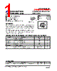

1. General Description & Features:
️· It's a MOSFET (likely N-Channel).
️· The datasheet outlines its electrical characteristics, thermal performance, and marking information.
️· It's designed for low on-resistance (RDS(on)), likely intended for efficiency in switching applications.
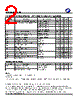
2. Absolute Maximum Ratings: (Not explicitly listed numerically, but implied by other characteristics)
️· Drain-Source Voltage (VDS) – Likely a value around 30V or higher, based on operating voltages mentioned elsewhere.
️· Gate-Source Voltage (VGS) - Likely a value around +/- 20V or more.
️· Drain Current (ID): A significant current handling capability.
️· Power Dissipation: Relatively high (implied by thermal characteristics).
️· Operating Temperature Range: Probably -40°C to 150°C.
️· Storage Temperature Range: A wider range.
3. Electrical Characteristics: (Many parameters listed, highlighting key ones)
️· RDS(on): A primary characteristic – very low, indicating good switching efficiency.
️· VGS(th): Gate-Source Threshold Voltage – a key parameter for determining when the MOSFET turns on.
️· Input Capacitance: Significant, implying switching considerations.
️· Output Capacitance: Another factor in switching performance.
️· Reverse Recovery Time: (For the body diode) – important for diode behavior.
4. Thermal Characteristics:
️· Thermal Resistance (RthJA, RthJC): Crucial for heat dissipation. RthJA is important for determining how the device behaves when mounted on a typical PCB, while RthJC is important to understand the local temperature behavior within the chip.
️· Safe Operating Area (SOA) graph: Defines the limits of safe operation in terms of voltage and current.
️· Transient Thermal Impedance graph: Illustrates how quickly the device temperature rises and falls.
5. Marking Information:
️· The datasheet explains how the part is marked, including:
- Part Number: MY
- Date Code: Based on year.
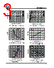
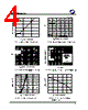
6. Graphs & Charts (Representing Key Data):
️· Transfer Characteristics
️· Drain Current vs. Ambient Temperature
️· Capacitance Characteristics
️· RDS(ON) vs. Temperature
️· Gate Charge Characteristics
7. Summary of Important Notes & Considerations:
️· RDS(ON) is low: This suggests the MOSFET is designed for power efficiency.
️· Thermal Management: Proper heat sinking and PCB layout are necessary due to the power dissipation.
️· Switching Speed: Input and output capacitances need to be considered when designing switching circuits.
️· SOA Limits: It is essential to operate within the specified safe operating area to prevent damage.
In essence, this datasheet provides all the necessary information for designing circuits that use the AP2323AGN-HF MOSFET, with an emphasis on efficient power switching applications.
1. General Description & Features:
️· It's a MOSFET (likely N-Channel).
️· The datasheet outlines its electrical characteristics, thermal performance, and marking information.
️· It's designed for low on-resistance (RDS(on)), likely intended for efficiency in switching applications.
2. Absolute Maximum Ratings: (Not explicitly listed numerically, but implied by other characteristics)
️· Drain-Source Voltage (VDS) – Likely a value around 30V or higher, based on operating voltages mentioned elsewhere.
️· Gate-Source Voltage (VGS) - Likely a value around +/- 20V or more.
️· Drain Current (ID): A significant current handling capability.
️· Power Dissipation: Relatively high (implied by thermal characteristics).
️· Operating Temperature Range: Probably -40°C to 150°C.
️· Storage Temperature Range: A wider range.
3. Electrical Characteristics: (Many parameters listed, highlighting key ones)
️· RDS(on): A primary characteristic – very low, indicating good switching efficiency.
️· VGS(th): Gate-Source Threshold Voltage – a key parameter for determining when the MOSFET turns on.
️· Input Capacitance: Significant, implying switching considerations.
️· Output Capacitance: Another factor in switching performance.
️· Reverse Recovery Time: (For the body diode) – important for diode behavior.
4. Thermal Characteristics:
️· Thermal Resistance (RthJA, RthJC): Crucial for heat dissipation. RthJA is important for determining how the device behaves when mounted on a typical PCB, while RthJC is important to understand the local temperature behavior within the chip.
️· Safe Operating Area (SOA) graph: Defines the limits of safe operation in terms of voltage and current.
️· Transient Thermal Impedance graph: Illustrates how quickly the device temperature rises and falls.
5. Marking Information:
️· The datasheet explains how the part is marked, including:
- Part Number: MY
- Date Code: Based on year.
6. Graphs & Charts (Representing Key Data):
️· Transfer Characteristics
️· Drain Current vs. Ambient Temperature
️· Capacitance Characteristics
️· RDS(ON) vs. Temperature
️· Gate Charge Characteristics
7. Summary of Important Notes & Considerations:
️· RDS(ON) is low: This suggests the MOSFET is designed for power efficiency.
️· Thermal Management: Proper heat sinking and PCB layout are necessary due to the power dissipation.
️· Switching Speed: Input and output capacitances need to be considered when designing switching circuits.
️· SOA Limits: It is essential to operate within the specified safe operating area to prevent damage.
In essence, this datasheet provides all the necessary information for designing circuits that use the AP2323AGN-HF MOSFET, with an emphasis on efficient power switching applications.
| Part No. | AP2323AGN-HF_16 |
| Manufacturer | A-POWER |
| Size | 102 Kbytes |
| Pages | 5 pages |
| Description | Small Package Outline |
| Does ALLDATASHEET help your business so far? [ DONATE ] |
About Alldatasheet | Advertisement | Contact us | Privacy Policy | Link to Datasheet | Link Exchange | Manufacturer List All Rights Reserved©Alldatasheet.com |
| Russian : Alldatasheetru.com | Korean : Alldatasheet.co.kr | Spanish : Alldatasheet.es | French : Alldatasheet.fr | Italian : Alldatasheetit.com Portuguese : Alldatasheetpt.com | Polish : Alldatasheet.pl | Vietnamese : Alldatasheet.vn Indian : Alldatasheet.in | Mexican : Alldatasheet.com.mx | British : Alldatasheet.co.uk | New Zealand : Alldatasheet.co.nz |
|
Family Site : ic2ic.com |
icmetro.com |
 Indian ▼
  English
 Chinese
 German
 Japanese
 Russian
 Korean
 Spanish
 French
 Italian
 Portuguese
 Polish
 Vietnamese
 Mexican
 British
 New Zealand