 |
Electronic Components Datasheet Search |
|
|
Electronic Components Datasheet Search |
|
The question interval is too short.
Please try again in a few seconds.

Hello, Please ask a question about LTM8032MPVPBF Datasheet
# Example questions:
➢ What is the purpose of the aux pin and how is it typically connected in a standard ltm8032 design?
➢ What is its function, and under what circumstances would it be utilized?
➢ Explain the function of the run/ss pin, including how it affects shutdown and soft-start operations.
| Part No. | LTM8032MPVPBF |
| Manufacturer | LINER |
| Size | 310 Kbytes |
| Pages | 20 pages |
| Description | Ultralow Noise EMC Compliant 36V, 2A DC/DC 關Module |

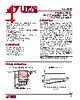


1. Overview & General Description:
️· Device: LTM8032
️· Type: DC-DC Converter (likely synchronous buck-boost, based on the information)
️· Function: A high-efficiency, dual-channel, synchronous buck-boost converter.
2. Key Features (Implied from text):
️· Dual-channel operation (two separate converters within the same chip)
️· Synchronous rectification (increased efficiency)
️· Burst Mode operation (for improved light-load efficiency)
️· Synchronizable (can be clocked to an external source)
️· Programmable switching frequency (using an external resistor)
️· Input voltage range: Not explicitly stated, but references to 36V imply a suitable range for that.
️· Output voltage regulation (0.79V reference)
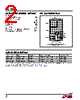
3. Pin Functions (Very Detailed List):
️· V<sub>IN</sub> (Bank 3): Input voltage supply – requires bypass capacitor.
️· F<sub>IN</sub> (K3, L3): Filtered Input – typically left unconnected unless specific EMI modification is needed.
️· GND (Bank 2): Ground connections - locally tied to a ground plane.
️· V<sub>OUT</sub> (Bank 1): Power output pins – where output filter capacitors and load connect.
️· AUX (Pin H5): Internal voltage source (connected to V<sub>OUT</sub>), used for BIAS pin.
️· BIAS (Pin H4): Requires voltage source greater than 2.8V. Connect to V<sub>OUT</sub> if output voltage > 2.8V. Otherwise connect to a voltage source between 2.8V and 25V.
️· RUN/SS (Pin L5): Shutdown control. Pull low to shut down. Tie to 2.5V or higher for normal operation. Provides soft-start functionality.
️· RT (Pin G7): Programming switching frequency (uses external resistor).
️· SHARE (Pin H7): Used when paralleling multiple LTM8032s.
️· SYNC (Pin L6): External clock synchronization. Ground for Burst Mode. Tie high to disable Burst Mode.
️· PGOOD (Pin K7): Output indicating regulation status (within 10% of regulation voltage).
️· ADJ (Pin J7): Regulates output voltage (0.79V reference). Used in feedback divider resistor calculation.
4. Equations & Design Considerations:
️· ADJ Resistor Calculation:
- `R_ADJ = (0.79 / (V_OUT - 0.79)) * 1000` (where `R_ADJ` is in kΩ)
5. Diagram and Circuit Considerations:
️· A detailed schematic diagram (labeled "8032fa") is included, illustrating the component placement and interconnections for a circuit example.
️· Emphasis on the use of capacitors and filter components.
6. Key Application Notes (Implied):
️· Input Filtering: Pay attention to input EMI filtering.
️· Grounding: Proper grounding is crucial for performance.
️· Soft-Start: The RUN/SS pin provides soft-start to reduce inrush current.
️· Parallel Operation: Sharing the load between multiple LTM8032s is possible.
What’s Missing (Potential Further Investigation):
️· Input Voltage Range: The exact operating voltage window is not explicitly given.
️· Output Current Capabilities: The maximum output current per channel isn't stated.
️· Detailed Specifications: Key electrical specifications (efficiency curves, voltage regulation accuracy, ripple voltage) would be found in the full datasheet.
1. Overview & General Description:
️· Device: LTM8032
️· Type: DC-DC Converter (likely synchronous buck-boost, based on the information)
️· Function: A high-efficiency, dual-channel, synchronous buck-boost converter.
2. Key Features (Implied from text):
️· Dual-channel operation (two separate converters within the same chip)
️· Synchronous rectification (increased efficiency)
️· Burst Mode operation (for improved light-load efficiency)
️· Synchronizable (can be clocked to an external source)
️· Programmable switching frequency (using an external resistor)
️· Input voltage range: Not explicitly stated, but references to 36V imply a suitable range for that.
️· Output voltage regulation (0.79V reference)
3. Pin Functions (Very Detailed List):
️· V<sub>IN</sub> (Bank 3): Input voltage supply – requires bypass capacitor.
️· F<sub>IN</sub> (K3, L3): Filtered Input – typically left unconnected unless specific EMI modification is needed.
️· GND (Bank 2): Ground connections - locally tied to a ground plane.
️· V<sub>OUT</sub> (Bank 1): Power output pins – where output filter capacitors and load connect.
️· AUX (Pin H5): Internal voltage source (connected to V<sub>OUT</sub>), used for BIAS pin.
️· BIAS (Pin H4): Requires voltage source greater than 2.8V. Connect to V<sub>OUT</sub> if output voltage > 2.8V. Otherwise connect to a voltage source between 2.8V and 25V.
️· RUN/SS (Pin L5): Shutdown control. Pull low to shut down. Tie to 2.5V or higher for normal operation. Provides soft-start functionality.
️· RT (Pin G7): Programming switching frequency (uses external resistor).
️· SHARE (Pin H7): Used when paralleling multiple LTM8032s.
️· SYNC (Pin L6): External clock synchronization. Ground for Burst Mode. Tie high to disable Burst Mode.
️· PGOOD (Pin K7): Output indicating regulation status (within 10% of regulation voltage).
️· ADJ (Pin J7): Regulates output voltage (0.79V reference). Used in feedback divider resistor calculation.
4. Equations & Design Considerations:
️· ADJ Resistor Calculation:
- `R_ADJ = (0.79 / (V_OUT - 0.79)) * 1000` (where `R_ADJ` is in kΩ)
5. Diagram and Circuit Considerations:
️· A detailed schematic diagram (labeled "8032fa") is included, illustrating the component placement and interconnections for a circuit example.
️· Emphasis on the use of capacitors and filter components.
6. Key Application Notes (Implied):
️· Input Filtering: Pay attention to input EMI filtering.
️· Grounding: Proper grounding is crucial for performance.
️· Soft-Start: The RUN/SS pin provides soft-start to reduce inrush current.
️· Parallel Operation: Sharing the load between multiple LTM8032s is possible.
What’s Missing (Potential Further Investigation):
️· Input Voltage Range: The exact operating voltage window is not explicitly given.
️· Output Current Capabilities: The maximum output current per channel isn't stated.
️· Detailed Specifications: Key electrical specifications (efficiency curves, voltage regulation accuracy, ripple voltage) would be found in the full datasheet.
| Part No. | LTM8032MPVPBF |
| Manufacturer | LINER |
| Size | 310 Kbytes |
| Pages | 20 pages |
| Description | Ultralow Noise EMC Compliant 36V, 2A DC/DC 關Module |
| Does ALLDATASHEET help your business so far? [ DONATE ] |
About Alldatasheet | Advertisement | Contact us | Privacy Policy | Link to Datasheet | Link Exchange | Manufacturer List All Rights Reserved©Alldatasheet.com |
| Russian : Alldatasheetru.com | Korean : Alldatasheet.co.kr | Spanish : Alldatasheet.es | French : Alldatasheet.fr | Italian : Alldatasheetit.com Portuguese : Alldatasheetpt.com | Polish : Alldatasheet.pl | Vietnamese : Alldatasheet.vn Indian : Alldatasheet.in | Mexican : Alldatasheet.com.mx | British : Alldatasheet.co.uk | New Zealand : Alldatasheet.co.nz |
|
Family Site : ic2ic.com |
icmetro.com |
 Indian ▼
  English
 Chinese
 German
 Japanese
 Russian
 Korean
 Spanish
 French
 Italian
 Portuguese
 Polish
 Vietnamese
 Mexican
 British
 New Zealand