 |
Electronic Components Datasheet Search |
|
|
Electronic Components Datasheet Search |
|
The question interval is too short.
Please try again in a few seconds.

Hello, Please ask a question about DMC3028LSDXQ Datasheet
# Example questions:
➢ What is the primary difference in the application of the 'p-channel – q2' versus the 'n-channel – q1' mosfets?
➢ Describe how temperature affects rds(on) for both the p-channel and n-channel mosfets, as shown in the graphs.
➢ Identify at least two parameters, besides voltage and current, that influence the characteristics of the mosfets based on the provided datasheet excerpts.
| Part No. | DMC3028LSDXQ |
| Manufacturer | DIODES |
| Size | 490 Kbytes |
| Pages | 9 pages |
| Description | COMPLEMENTARY PAIR ENHANCEMENT MODE MOSFET |




1. General Information:
️· Part Number: DMC3028LSDXQ
️· Type: MOSFET (Metal-Oxide-Semiconductor Field-Effect Transistor) - Available in both N-Channel (Q1) and P-Channel (Q2) variants.
️· Datasheet Revision: Rev. 1 - 2
2. N-Channel (Q1) Characteristics:
️· Voltage/Current:
- Drain-Source Voltage (Vds): Likely supports voltages up to ~30V.
- Drain Current (Id): Supports currents up to ~ -10A, at least in typical testing conditions.
- Gate-Source Voltage (Vgs): Typical gate voltage ranges from -10V to -4.5V
️· Electrical Behavior:
- On-Resistance (Rds(on)): The datasheet provides graphs showing how Rds(on) varies with gate-source voltage (Vgs) and junction temperature. From the graphs, it appears relatively low resistance in the active region.
- Junction Capacitance: Exhibits junction capacitance behavior, see Figure 10.
- Leakage Current: Figure 9 depicts how leakage current changes as a function of drain-source voltage (Vds).
️· Key Features (Based on graphs):
- Fast Switching: Graphically suggested by characteristics shown in Figure 11.
3. P-Channel (Q2) Characteristics:
️· Voltage/Current:
- Drain-Source Voltage (Vds): Likely supports voltages up to ~30V.
- Drain Current (Id): Supports currents up to ~10A
- Gate-Source Voltage (Vgs): Typical gate voltage ranges from 5V to -4.5V
️· Electrical Behavior:
- On-Resistance (Rds(on)): The datasheet provides graphs showing how Rds(on) varies with gate-source voltage (Vgs) and junction temperature. From the graphs, it appears relatively low resistance in the active region.
- Junction Capacitance: Exhibits junction capacitance behavior, see Figure 10.
- Leakage Current: Figure 11 depicts how leakage current changes as a function of drain-source voltage (Vds).
️· Key Features (Based on graphs):
- Fast Switching: Graphically suggested by characteristics shown in Figure 11.
4. Figures and Graphs (Key Insights):
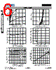
️· Figure 1 (Output Characteristics): Shows the relationship between drain current (Id) and drain-source voltage (Vds) for different gate-source voltages (Vgs).
️· Figure 3 (On-Resistance vs. Current): Displays how on-resistance changes with drain current for both channels.
️· Figure 4 (On-Resistance vs. Vgs): Illustrates the relationship between on-resistance and gate-source voltage.
️· Figure 8 (Diode Forward Voltage vs. Current): Shows the forward voltage characteristics when used as a diode.
️· Figure 11 (Total Gate Charge vs. Vgs): Useful for understanding gate drive requirements.
️· Figure 10 (Junction Capacitance): Information useful for high-frequency circuit design.
Important Notes & Limitations:
️· Missing Values: Many specific numerical values for parameters are not explicitly provided in the provided text. This would typically be found in a standard datasheet.
️· Graphical Interpretation: Some information has been inferred from the graphs. A full interpretation would require more detailed analysis and potentially plotting of data points from the graphs.
️· Conditions: Remember that all electrical characteristics are dependent on temperature, voltage, and other conditions.
️· Complete Datasheet: This summary is based only on the provided text. For proper design, a full datasheet is essential.
1. General Information:
️· Part Number: DMC3028LSDXQ
️· Type: MOSFET (Metal-Oxide-Semiconductor Field-Effect Transistor) - Available in both N-Channel (Q1) and P-Channel (Q2) variants.
️· Datasheet Revision: Rev. 1 - 2
2. N-Channel (Q1) Characteristics:
️· Voltage/Current:
- Drain-Source Voltage (Vds): Likely supports voltages up to ~30V.
- Drain Current (Id): Supports currents up to ~ -10A, at least in typical testing conditions.
- Gate-Source Voltage (Vgs): Typical gate voltage ranges from -10V to -4.5V
️· Electrical Behavior:
- On-Resistance (Rds(on)): The datasheet provides graphs showing how Rds(on) varies with gate-source voltage (Vgs) and junction temperature. From the graphs, it appears relatively low resistance in the active region.
- Junction Capacitance: Exhibits junction capacitance behavior, see Figure 10.
- Leakage Current: Figure 9 depicts how leakage current changes as a function of drain-source voltage (Vds).
️· Key Features (Based on graphs):
- Fast Switching: Graphically suggested by characteristics shown in Figure 11.
3. P-Channel (Q2) Characteristics:
️· Voltage/Current:
- Drain-Source Voltage (Vds): Likely supports voltages up to ~30V.
- Drain Current (Id): Supports currents up to ~10A
- Gate-Source Voltage (Vgs): Typical gate voltage ranges from 5V to -4.5V
️· Electrical Behavior:
- On-Resistance (Rds(on)): The datasheet provides graphs showing how Rds(on) varies with gate-source voltage (Vgs) and junction temperature. From the graphs, it appears relatively low resistance in the active region.
- Junction Capacitance: Exhibits junction capacitance behavior, see Figure 10.
- Leakage Current: Figure 11 depicts how leakage current changes as a function of drain-source voltage (Vds).
️· Key Features (Based on graphs):
- Fast Switching: Graphically suggested by characteristics shown in Figure 11.
4. Figures and Graphs (Key Insights):
️· Figure 1 (Output Characteristics): Shows the relationship between drain current (Id) and drain-source voltage (Vds) for different gate-source voltages (Vgs).
️· Figure 3 (On-Resistance vs. Current): Displays how on-resistance changes with drain current for both channels.
️· Figure 4 (On-Resistance vs. Vgs): Illustrates the relationship between on-resistance and gate-source voltage.
️· Figure 8 (Diode Forward Voltage vs. Current): Shows the forward voltage characteristics when used as a diode.
️· Figure 11 (Total Gate Charge vs. Vgs): Useful for understanding gate drive requirements.
️· Figure 10 (Junction Capacitance): Information useful for high-frequency circuit design.
Important Notes & Limitations:
️· Missing Values: Many specific numerical values for parameters are not explicitly provided in the provided text. This would typically be found in a standard datasheet.
️· Graphical Interpretation: Some information has been inferred from the graphs. A full interpretation would require more detailed analysis and potentially plotting of data points from the graphs.
️· Conditions: Remember that all electrical characteristics are dependent on temperature, voltage, and other conditions.
️· Complete Datasheet: This summary is based only on the provided text. For proper design, a full datasheet is essential.
| Part No. | DMC3028LSDXQ |
| Manufacturer | DIODES |
| Size | 490 Kbytes |
| Pages | 9 pages |
| Description | COMPLEMENTARY PAIR ENHANCEMENT MODE MOSFET |
| Does ALLDATASHEET help your business so far? [ DONATE ] |
About Alldatasheet | Advertisement | Contact us | Privacy Policy | Link to Datasheet | Link Exchange | Manufacturer List All Rights Reserved©Alldatasheet.com |
| Russian : Alldatasheetru.com | Korean : Alldatasheet.co.kr | Spanish : Alldatasheet.es | French : Alldatasheet.fr | Italian : Alldatasheetit.com Portuguese : Alldatasheetpt.com | Polish : Alldatasheet.pl | Vietnamese : Alldatasheet.vn Indian : Alldatasheet.in | Mexican : Alldatasheet.com.mx | British : Alldatasheet.co.uk | New Zealand : Alldatasheet.co.nz |
|
Family Site : ic2ic.com |
icmetro.com |
 Indian ▼
  English
 Chinese
 German
 Japanese
 Russian
 Korean
 Spanish
 French
 Italian
 Portuguese
 Polish
 Vietnamese
 Mexican
 British
 New Zealand