|
Electronic Components Datasheet Search |
|
|
Electronic Components Datasheet Search |
|
ADA4940-1ACPZ-R2 Datasheet(PDF) 21 Page - Analog Devices |
|
|
|||||||||||||||||||||||||||||
ADA4940-1ACPZ-R2 Datasheet(HTML) 21 Page - Analog Devices |
|
|
21 / 30 page 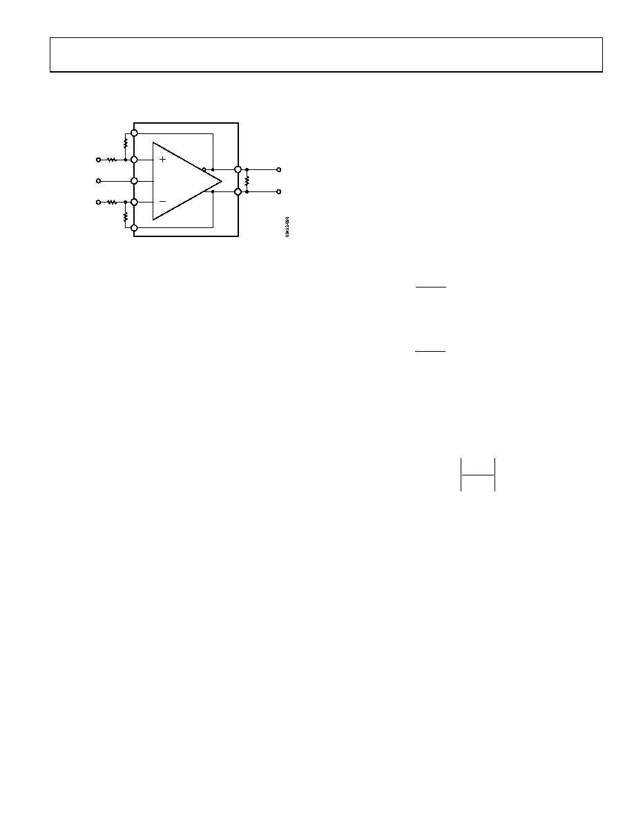 Data Sheet ADA4940-1/ADA4940-2 Rev. E | Page 21 of 30 TERMINOLOGY DEFINITION OF TERMS ADA4940-1/ ADA4940-2 RL, dm VOUT, dm RF RF RG RG +FB +IN +OUT –OUT – + +DIN +VOCM –DIN –FB –IN Figure 61. Circuit Definitions Differential Voltage Differential voltage refers to the difference between two node voltages. For example, the differential output voltage (or equivalently, output differential mode voltage) is defined as VOUT, dm = (V+OUT − V−OUT) where V+OUT and V−OUT refer to the voltages at the +OUT and −OUT terminals with respect to a common reference. Similarly, the differential input voltage is defined as VIN, dm = (+DIN − (−DIN)) Common-Mode Voltage (CMV) CMV refers to the average of two node voltages. The output common-mode voltage is defined as VOUT, cm = (V+OUT + V−OUT)/2 Similarly, the input common-mode voltage is defined as VIN, cm = (+DIN + (−DIN))/2 Common-Mode Offset Voltage The common-mode offset voltage is defined as the difference between the voltage applied to the VOCM terminal and the common mode of the output voltage. VOS, cm = VOUT, cm − VOCM Differential VOS, Differential CMRR, and VOCM CMRR The differential mode and common-mode voltages each have their own error sources. The differential offset (VOS, dm) is the voltage error between the +IN and −IN terminals of the amplifier. Differential CMRR reflects the change of VOS, dm in response to changes to the common-mode voltage at the input terminals +DIN and −DIN. dm OS, cm IN, DIFF ΔV ΔV CMRR = VOCM CMRR reflects the change of VOS, dm in response to changes to the common-mode voltage at the output terminals. dm OS, OCM V ΔV ΔV CMRR OCM = Balance Balance is a measure of how well the differential signals are matched in amplitude; the differential signals are exactly 180° apart in phase. By this definition, the output balance is the magnitude of the output common-mode voltage divided by the magnitude of the output differential mode voltage. dm OUT cm OUT V V Error Balance Output , , = |
|
Link URL |
| Does ALLDATASHEET help your business so far? [ DONATE ] |
About Alldatasheet | Advertisement | Contact us | Privacy Policy | Link to Datasheet | Link Exchange | Manufacturer List All Rights Reserved©Alldatasheet.com |
| Russian : Alldatasheetru.com | Korean : Alldatasheet.co.kr | Spanish : Alldatasheet.es | French : Alldatasheet.fr | Italian : Alldatasheetit.com Portuguese : Alldatasheetpt.com | Polish : Alldatasheet.pl | Vietnamese : Alldatasheet.vn Indian : Alldatasheet.in | Mexican : Alldatasheet.com.mx | British : Alldatasheet.co.uk | New Zealand : Alldatasheet.co.nz |
|
Family Site : ic2ic.com |
icmetro.com |
 Indian ▼
 English
 Chinese
 German
 Japanese
 Russian
 Korean
 Spanish
 French
 Italian
 Portuguese
 Polish
 Vietnamese
 Indian
 Mexican
 British
 New Zealand