|
Electronic Components Datasheet Search |
|
|
Electronic Components Datasheet Search |
|
AD8422ARMZ-R7 Datasheet(PDF) 24 Page - Analog Devices |
|
|
|||||||||||||||||||||||||||||
AD8422ARMZ-R7 Datasheet(HTML) 24 Page - Analog Devices |
|
|
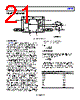
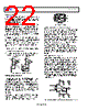
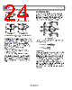
24 / 27 page 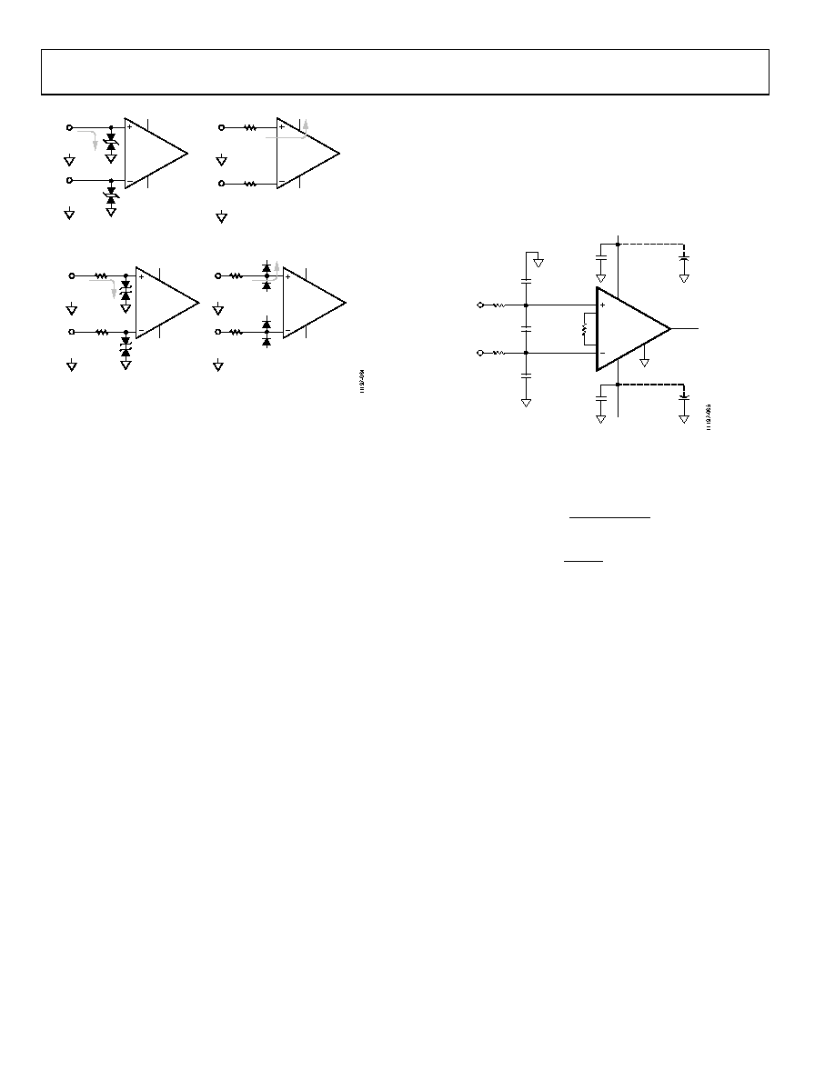 AD8422 Data Sheet Rev. B | Page 24 of 27 +VS AD8422 –VS VIN+ + – VIN– + – +VS AD8422 RPROTECT RPROTECT –VS I VIN+ + – VIN– + – +VS +VS AD8422 RPROTECT RPROTECT –VS –VS I VIN+ + – VIN– + – +VS –VS +VS AD8422 RPROTECT RPROTECT –VS I VIN+ + – VIN– + – I SIMPLE CONTINUOUS PROTECTION TRANSIENT PROTECTION LOW NOISE CONTINUOUS OPTION 2 LOW NOISE CONTINUOUS OPTION 1 Figure 62. Input Protection Options for Input Voltages Beyond Absolute Maximum Ratings At the expense of some noise performance, another solution is to use series resistors. In the overvoltage case, current into the inputs of the AD8422 is internally limited to a safe value for the amplifier. Although the AD8422 inputs must still be kept within the Absolute Maximum Ratings, the I × R drop across the protection resistor increases the maximum voltage that the system can withstand to the following values: For positive input signals, VMAX_NEW = (40 V + Negative Supply) + IIN × RPROTECT For negative input signals, VMIN_NEW = (Positive Supply – 40 V) − IOUT × RPROTECT Overvoltage performance is shown in Figure 15, Figure 16, Figure 17, and Figure 18. With gains greater than 100 and supply voltages less than ±2.5 V, overdrive voltages beyond the rails may cause the output to invert as far as the REF pin voltage. RF INTERFERENCE (RFI) RF rectification is often a problem when amplifiers are used in applications that have strong RF signals. The disturbance can appear as a small dc offset voltage. High frequency signals can be filtered with a low-pass RC network placed at the input of the instrumentation amplifier, as shown in Figure 63. R R AD8422 +VS +IN –IN 0.1µF 10µF 10µF 0.1µF REF VOUT –VS RG CD 10nF CC 1nF CC 1nF 2kΩ 2kΩ Figure 63. RFI Suppression The filter limits the input signal bandwidth, according to the following relationship: ) 2 ( π 2 1 C D DIFF C C R uency FilterFreq + = C CM RC uency FilterFreq π 2 1 = where CD ≥ 10 CC. CD affects the difference signal, and CC affects the common-mode signal. Choose values of R and CC that minimize RFI. A mismatch between R × CC at the positive input and R × CC at the negative input degrades the CMRR of the AD8422. By using a value of CD that is one order of magnitude larger than CC, the effect of the mismatch is reduced, and performance is improved. Resistors add noise; therefore, the choice of the resistor and capacitor values depends on the desired tradeoff between noise, input impedance at high frequencies, and RF immunity. The resistors used for the RFI filter can be the same as those used for input protection. |
|
Link URL |
| Does ALLDATASHEET help your business so far? [ DONATE ] |
About Alldatasheet | Advertisement | Contact us | Privacy Policy | Link to Datasheet | Link Exchange | Manufacturer List All Rights Reserved©Alldatasheet.com |
| Russian : Alldatasheetru.com | Korean : Alldatasheet.co.kr | Spanish : Alldatasheet.es | French : Alldatasheet.fr | Italian : Alldatasheetit.com Portuguese : Alldatasheetpt.com | Polish : Alldatasheet.pl | Vietnamese : Alldatasheet.vn Indian : Alldatasheet.in | Mexican : Alldatasheet.com.mx | British : Alldatasheet.co.uk | New Zealand : Alldatasheet.co.nz |
|
Family Site : ic2ic.com |
icmetro.com |
 Indian ▼
 English
 Chinese
 German
 Japanese
 Russian
 Korean
 Spanish
 French
 Italian
 Portuguese
 Polish
 Vietnamese
 Indian
 Mexican
 British
 New Zealand