13 / 14 page
13 of 14
RF2361
Rev A10 DS070731
7628 Thorndike Road, Greensboro, NC 27409-9421 · For sales or technical
support, contact RFMD at (+1) 336-678-5570 or sales-support@rfmd.com.
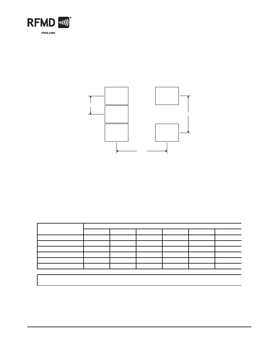
PCB Solder Mask Pattern
Liquid Photo-Imageable (LPI) solder mask is recommended. The solder mask footprint will match what is shown for the PCB
metal land pattern with a 2mil to 3mil expansion to accommodate solder mask registration clearance around all pads. The
center-grounding pad shall also have a solder mask clearance. Expansion of the pads to create solder mask clearance can be
provided in the master data or requested from the PCB fabrication supplier.
A
A
A
A
A
2.60
Pin 1
A = 0.90 x 1.20 (mm) Typ.
Pin 5
Dimensions in mm.
0.95 Typ.
1.90 Typ.
Figure 2. PCB Solder Mask (Top View)
RoHS Compliant:
No
Package total weight in gram
0.015
Compliance Date Code:
N/A
Bill of Materials Revision:
Rev-
Pb Free Category:
Contains Pb
Pb
Cd
Hg
Cr VI
PB B
PB DE
Di e
00
000
0
Mol di ng Compo und
00
000
0
Lead F r ame
00
000
0
Di e Attach Epo x y
00
000
0
Wi r e
00
000
0
So l der Pl ati ng
4753
0
0
0
0
0
* DIRECTIVE 2002/95/EC OF THE EUROPEAN PARLIAMENT AND OF THE COUNCIL of 27 January 2003 on the restriction of the
use of certain hazardous substances in electrical and electronic equipment
RoHS* Banned Material Content
B i ll o f Mate r i al s
Par ts Per Mi l l i on (PPM)
This R oHS banned mate r i al co nte nt de cl ar atio n was pr epar e d sole ly o n info r matio n, incl uding anal ytical
data, pr ovi de d to R F MD by i ts suppl i er s, and appl i e s to the B i l l of Mate r i al s (B OM) r evi si on note d

 Indian ▼
 English
 Chinese
 German
 Japanese
 Russian
 Korean
 Spanish
 French
 Italian
 Portuguese
 Polish
 Vietnamese
 Indian
 Mexican
 British
 New Zealand


