|
Electronic Components Datasheet Search |
|
|
Electronic Components Datasheet Search |
|
ADP7159ACPZ-04-R7 Datasheet(PDF) 17 Page - Analog Devices |
|
|
|||||||||||||||||||||||||||||
ADP7159ACPZ-04-R7 Datasheet(HTML) 17 Page - Analog Devices |
|
|
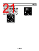
17 / 23 page  Data Sheet ADP7159 Rev. B | Page 17 of 23 START-UP TIME The ADP7159 uses an internal soft start to limit the inrush current when the output is enabled. The start-up time for a 3.3 V output is approximately 1.2 ms from the time the EN active threshold is crossed to when the output reaches 90% of its final value. The rise time in seconds of the output voltage (10% to 90%) is approximately 0.0012 × CBYP, where CBYP is in microfarads. 0 0.5 1.0 1.5 2.0 2.5 3.0 3.5 2 4 6 8 10 12 14 16 18 20 TIME (ms) –2 0 EN 1µF 4.7µF 10µF Figure 53. Typical Start-Up Behavior with CBYP = 1 µF to 10 µF 0 0.5 1.0 1.5 2.0 2.5 3.0 3.5 20 40 60 80 100 120 140 160 TIME (ms) EN 10µF 47µF 100µF –20 0 Figure 54. Typical Start-Up Behavior with CBYP = 10 µF to 100 µF REF, BYP, AND VREG PINS REF, BYP, and VREG generate voltages internally (VREF, VBYP, and VREG) that require external bypass capacitors for proper operation. Do not, under any circumstances, connect any loads to these pins, because doing so compromises the noise and PSRR performance of the ADP7159. Using larger values of CBYP, CREF, and CREG is acceptable but can increase the start-up time, as described in the Start-Up Time section. CURRENT-LIMIT AND THERMAL SHUTDOWN The ADP7159 is protected against damage due to excessive power dissipation by current and thermal overload protection circuits. The ADP7159 is designed to current limit when the output load reaches 3 A (typical). When the output load exceeds 3 A, the output voltage is reduced to maintain a constant current limit. When the ADP7159 junction temperature exceeds 150°C, the thermal shutdown circuit turns off the output voltage, reducing the output current to zero. Extreme junction temperature can be the result of high current operation, poor circuit board design, or high ambient temperature. A 15°C hysteresis is included so that the ADP7159 does not return to operation after thermal shutdown until the on-chip temperature falls below 135°C. When the device exits thermal shutdown, a soft start is initiated to reduce the inrush current. Current limit and thermal shutdown protections are intended to protect the device against accidental overload conditions. Cases with a hard short from VOUT to ground or an extremely long soft-start timer typically cause the device to experience thermal oscillations between the current limit and thermal shutdown. THERMAL CONSIDERATIONS In applications with a low input to output voltage differential, the ADP7159 does not dissipate much heat. However, in applications with high ambient temperature and/or high input voltage, the heat dissipated in the package can become large enough that it causes the junction temperature of the die to exceed the maximum junction temperature of 125°C. The junction temperature of the die is the sum of the ambient temperature of the environment and the temperature rise of the package due to the power dissipation, as shown in Equation 2. To guarantee reliable operation, the junction temperature of the ADP7159 must not exceed 125°C. To ensure that the junction temperature stays below this maximum value, the user must be aware of the parameters that contribute to junction temperature changes. These parameters include ambient temperature, power dissipation in the power device, and thermal resistances between the junction temperature and ambient air (θJA). The θJA number is dependent on the package assembly compounds used, as well as the amount of copper used to solder the package ground and the exposed pad to the PCB. |
|
|
Link URL |
| Does ALLDATASHEET help your business so far? [ DONATE ] |
About Alldatasheet | Advertisement | Contact us | Privacy Policy | Link to Datasheet | Link Exchange | Manufacturer List All Rights Reserved©Alldatasheet.com |
| Russian : Alldatasheetru.com | Korean : Alldatasheet.co.kr | Spanish : Alldatasheet.es | French : Alldatasheet.fr | Italian : Alldatasheetit.com Portuguese : Alldatasheetpt.com | Polish : Alldatasheet.pl | Vietnamese : Alldatasheet.vn Indian : Alldatasheet.in | Mexican : Alldatasheet.com.mx | British : Alldatasheet.co.uk | New Zealand : Alldatasheet.co.nz |
|
Family Site : ic2ic.com |
icmetro.com |
 Indian ▼
 English
 Chinese
 German
 Japanese
 Russian
 Korean
 Spanish
 French
 Italian
 Portuguese
 Polish
 Vietnamese
 Indian
 Mexican
 British
 New Zealand