 |
Electronic Components Datasheet Search |
|
|
Electronic Components Datasheet Search |
|
ADA4859-3ACPZ-R7 Datasheet(PDF) 5 Page - Analog Devices |
|
|
|||||||||||||||||||||||||||||
ADA4859-3ACPZ-R7 Datasheet(HTML) 5 Page - Analog Devices |
|
|
5 / 16 page 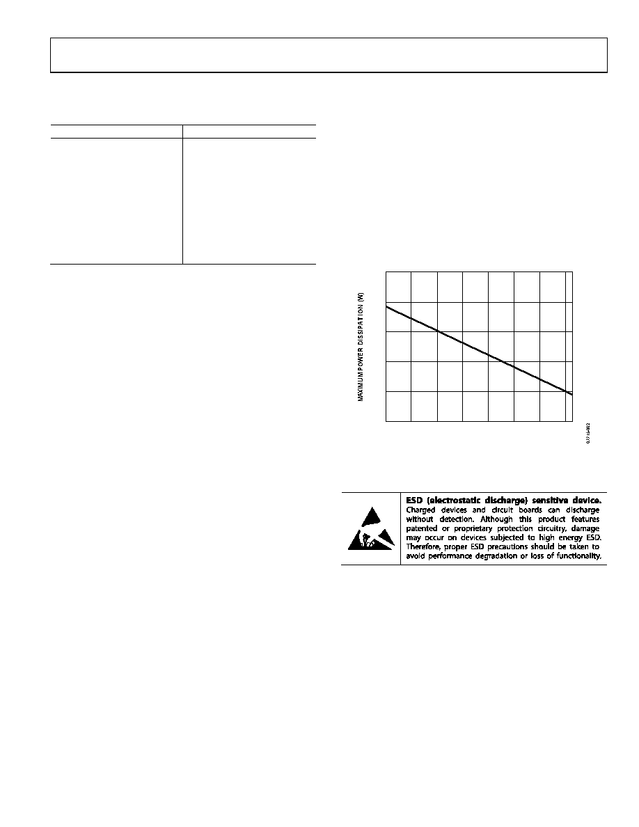 ADA4859-3 Rev. 0 | Page 5 of 16 ABSOLUTE MAXIMUM RATINGS MAXIMUM POWER DISSIPATION Table 3. The maximum power that can be safely dissipated by the ADA4859-3 is limited by the associated rise in junction temperature. The maximum safe junction temperature for plastic encapsulated devices is determined by the glass transition temperature of the plastic, approximately 150°C. Temporarily exceeding this limit may cause a shift in parametric performance due to a change in the stresses exerted on the die by the package. Exceeding a junction temperature of 175°C for an extended period can result in device failure. Parameter Rating Supply Voltage 6 V Internal Power Dissipation1 16-Lead LFCSP See Figure 2 Input Voltage (Common-Mode) (−VS − 0.2 V) to (+VS − 1.8 V) Differential Input Voltage ±VS Output Short-Circuit Duration Observe power derating curves Storage Temperature Range −65°C to +125°C Operating Temperature Range −40°C to +105°C Lead Temperature (Soldering, 10 sec) 300°C To ensure proper operation, it is necessary to observe the maximum power derating curves in Figure 2. 2.5 2.0 1.5 1.0 0.5 0 –40 –20 0 20 40 60 80 100 AMBIENT TEMPERATURE (°C) 1 Specification is for device in free air. Stresses above those listed under Absolute Maximum Ratings may cause permanent damage to the device. This is a stress rating only; functional operation of the device at these or any other conditions above those indicated in the operational section of this specification is not implied. Exposure to absolute maximum rating conditions for extended periods may affect device reliability. Figure 2. Maximum Power Dissipation vs. Ambient Temperature ESD CAUTION |
|
|
Link URL |
| Does ALLDATASHEET help your business so far? [ DONATE ] |
About Alldatasheet | Advertisement | Contact us | Privacy Policy | Link to Datasheet | Link Exchange | Manufacturer List All Rights Reserved©Alldatasheet.com |
| Russian : Alldatasheetru.com | Korean : Alldatasheet.co.kr | Spanish : Alldatasheet.es | French : Alldatasheet.fr | Italian : Alldatasheetit.com Portuguese : Alldatasheetpt.com | Polish : Alldatasheet.pl | Vietnamese : Alldatasheet.vn Indian : Alldatasheet.in | Mexican : Alldatasheet.com.mx | British : Alldatasheet.co.uk | New Zealand : Alldatasheet.co.nz |
|
Family Site : ic2ic.com |
icmetro.com |
 Indian ▼
 English
 Chinese
 German
 Japanese
 Russian
 Korean
 Spanish
 French
 Italian
 Portuguese
 Polish
 Vietnamese
 Indian
 Mexican
 British
 New Zealand


