|
Electronic Components Datasheet Search |
|
|
Electronic Components Datasheet Search |
|
M95160-R Datasheet(PDF) 19 Page - STMicroelectronics |
|
|
|||||||||||||||||||||||||||||
M95160-R Datasheet(HTML) 19 Page - STMicroelectronics |
|
|
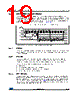
19 / 47 page 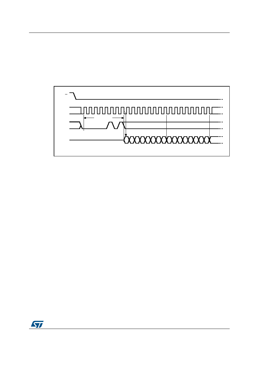 DocID022580 Rev 4 19/47 M95160 M95160-W M95160-R M95160-DF Instructions 46 6.3 Read Status Register (RDSR) The Read Status Register (RDSR) instruction is used to read the Status Register. The Status Register may be read at any time, even while a Write or Write Status Register cycle is in progress. When one of these cycles is in progress, it is recommended to check the Write In Progress (WIP) bit before sending a new instruction to the device. It is also possible to read the Status Register continuously, as shown in Figure 10. Figure 10. Read Status Register (RDSR) sequence The status and control bits of the Status Register are as follows: 6.3.1 WIP bit The Write In Progress (WIP) bit indicates whether the memory is busy with a Write or Write Status Register cycle. When set to 1, such a cycle is in progress, when reset to 0, no such cycle is in progress. 6.3.2 WEL bit The Write Enable Latch (WEL) bit indicates the status of the internal Write Enable Latch. When set to 1, the internal Write Enable Latch is set. When set to 0, the internal Write Enable Latch is reset, and no Write or Write Status Register instruction is accepted. The WEL bit is returned to its reset state by the following events: • Power-up • Write Disable (WRDI) instruction completion • Write Status Register (WRSR) instruction completion • Write (WRITE) instruction completion 6.3.3 BP1, BP0 bits The Block Protect (BP1, BP0) bits are non volatile. They define the size of the area to be software-protected against Write instructions. These bits are written with the Write Status Register (WRSR) instruction. When one or both of the Block Protect (BP1, BP0) bits is set to 1, the relevant memory area (as defined in Table 2) becomes protected against Write (WRITE) instructions. The Block Protect (BP1, BP0) bits can be written provided that the Hardware Protected mode has not been set. C D S 2 1 3456789 10 11 12 13 14 15 Instruction 0 AI02031E Q 7 6543210 Status Register Out High Impedance MSB 7 6543210 Status Register Out MSB 7 |
|
Link URL |
| Does ALLDATASHEET help your business so far? [ DONATE ] |
About Alldatasheet | Advertisement | Contact us | Privacy Policy | Link to Datasheet | Link Exchange | Manufacturer List All Rights Reserved©Alldatasheet.com |
| Russian : Alldatasheetru.com | Korean : Alldatasheet.co.kr | Spanish : Alldatasheet.es | French : Alldatasheet.fr | Italian : Alldatasheetit.com Portuguese : Alldatasheetpt.com | Polish : Alldatasheet.pl | Vietnamese : Alldatasheet.vn Indian : Alldatasheet.in | Mexican : Alldatasheet.com.mx | British : Alldatasheet.co.uk | New Zealand : Alldatasheet.co.nz |
|
Family Site : ic2ic.com |
icmetro.com |
 Indian ▼
 English
 Chinese
 German
 Japanese
 Russian
 Korean
 Spanish
 French
 Italian
 Portuguese
 Polish
 Vietnamese
 Indian
 Mexican
 British
 New Zealand