|
Electronic Components Datasheet Search |
|
|
Electronic Components Datasheet Search |
|
LP3311 Datasheet(PDF) 6 Page - Lowpower Semiconductor inc |
|
|
|||||||||||||||||||||||||||||
LP3311 Datasheet(HTML) 6 Page - Lowpower Semiconductor inc |
|
|
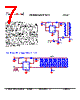
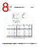
6 / 8 page  Preliminary Datasheet LP3311 LP3311 – 00 Version 1.0 Datasheet Feb.-2011 www.lowpowersemi.com Page 6 of 8 Applications Information LED Current Control The LP3311 regulates the LED current by setting the current sense resistor (R1) connecting to feedback and ground. The internal feedback reference voltage is 200mV or LP3311A is 300mV. The LED current can be set from following equation easily. ILED=200mV/R1 (LP3311) ILED=300mV/R1 (LP3311A) In order to have an accurate LED current, precision resistors are preferred (1% is recommended). The table for R1 selection is shown below. Inductor Selection The recommended value of inductor for 2 to 10 WLEDs applications are 2.2 to 22µH. Small size and better efficiency are the major concerns for portable device, such as LP3311 used for mobile phone. The inductor should have low core loss at 1.3MHz and low DCR for better efficiency. To avoid inductor saturation current rating should be considered. Dimming control a. Using a PWM Signal to EN Pin For controlling the LED brightness, the LP3311 can perform the dimming control by applying a PWM signal to EN pin. The internal soft-start and wide range dimming frequency from 100Hz to 100KHz can insignificantly reduce audio noise when dimming. The average LED current is proportional to the PWM signal duty cycle. The magnitude of the PWM signal should be higher than the maximum enable voltage of EN pin, in order to let the dimming control perform correctly. Cout 1uF 4.7uH Cin 10uF R1 10 Vin EN 4 FB 3 Vin 6 OVP 5 LP3311 PWM b. Using a DC Voltage Using a variable DC voltage to adjust the brightness is a popular method in some applications. The dimming control using a DC voltage circuit is shown in Figure 4. According to the Superposition Theorem, as the DC voltage increases, the voltage contributed to VFB increases and the voltage drop on R2 decreases, i.e. the LED current decreases. For example, if the VDC range is from 0V to 2.8V, the selection of resistors in Figure 4 sets dimming control of LED current from 20mA to 0mA. Cout 1uF 4.7uH Cin 10uF R1 10 Vin EN 4 FB 3 Vin 6 OVP 5 U4 LP3311 R2 5k R3 90k VDC |
|
|
Link URL |
| Does ALLDATASHEET help your business so far? [ DONATE ] |
About Alldatasheet | Advertisement | Contact us | Privacy Policy | Link to Datasheet | Link Exchange | Manufacturer List All Rights Reserved©Alldatasheet.com |
| Russian : Alldatasheetru.com | Korean : Alldatasheet.co.kr | Spanish : Alldatasheet.es | French : Alldatasheet.fr | Italian : Alldatasheetit.com Portuguese : Alldatasheetpt.com | Polish : Alldatasheet.pl | Vietnamese : Alldatasheet.vn Indian : Alldatasheet.in | Mexican : Alldatasheet.com.mx | British : Alldatasheet.co.uk | New Zealand : Alldatasheet.co.nz |
|
Family Site : ic2ic.com |
icmetro.com |
 Indian ▼
 English
 Chinese
 German
 Japanese
 Russian
 Korean
 Spanish
 French
 Italian
 Portuguese
 Polish
 Vietnamese
 Indian
 Mexican
 British
 New Zealand