|
Electronic Components Datasheet Search |
|
|
Electronic Components Datasheet Search |
|
AD8422ARZ-R7 Datasheet(PDF) 22 Page - Analog Devices |
|
|
|||||||||||||||||||||||||||||
AD8422ARZ-R7 Datasheet(HTML) 22 Page - Analog Devices |
|
|
22 / 25 page 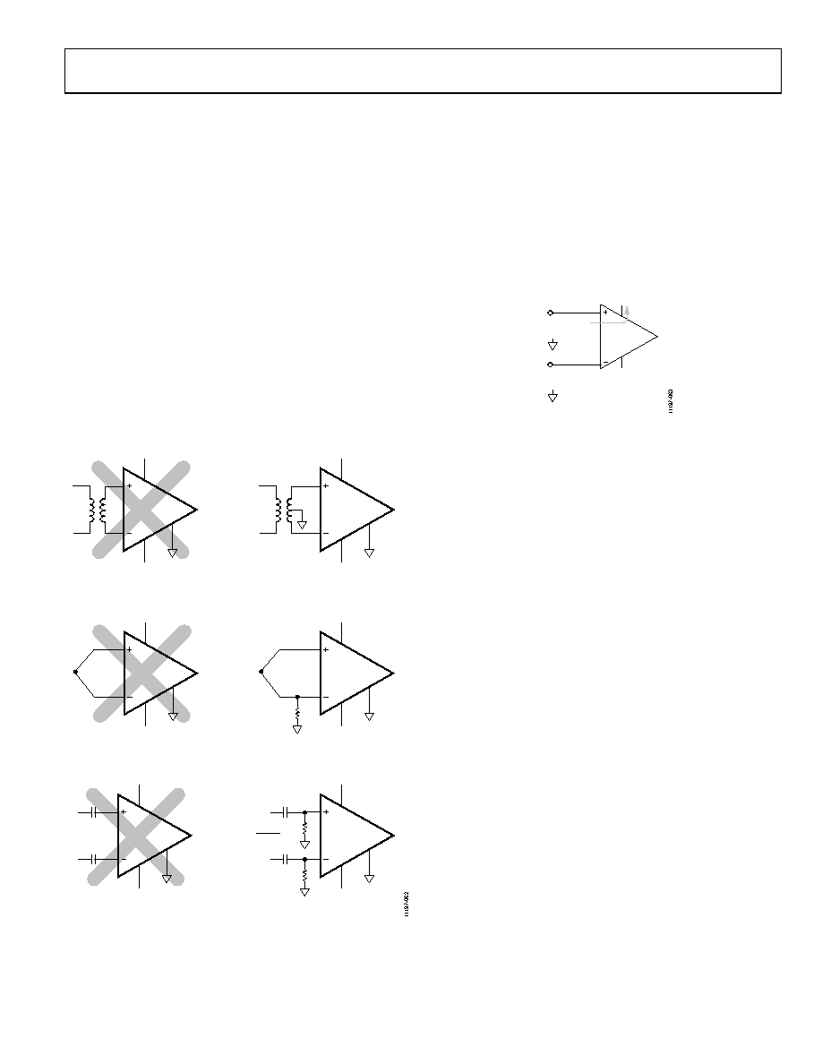 Data Sheet AD8422 A ground plane layer is helpful to reduce parasitic inductances. This minimizes voltage drops with changes in current. The area of the current path is directly proportional to the magnitude of parasitic inductances and, therefore, the impedance of the path at high frequencies. Large changes in currents in an inductive decoupling path or ground return create unwanted effects due to the coupling of such changes into the amplifier inputs. Because load currents flow from the supplies, connect the load at the same physical location as the bypass capacitor grounds. Reference Pin The output voltage of the AD8422 is developed with respect to the potential on the reference terminal. Ensure that REF is tied to the appropriate local ground. INPUT BIAS CURRENT RETURN PATH The input bias current of the AD8422 must have a dc return path to ground. When using a floating source without a current return path, such as a thermocouple, create a current return path, as shown in Figure 59. THERMOCOUPLE +VS REF –VS AD8422 CAPACITIVELY COUPLED +VS REF C C –VS AD8422 TRANSFORMER +VS REF –VS AD8422 INCORRECT CAPACITIVELY COUPLED +VS REF C R R C –VS AD8422 1 fHIGH-PASS = 2πRC THERMOCOUPLE +VS REF –VS 10MΩ AD8422 TRANSFORMER +VS REF –VS AD8422 CORRECT Figure 59. Creating an Input Bias Current Return Path INPUT VOLTAGES BEYOND THE SUPPLY RAILS Many instrumentation amplifiers specify excellent CMRR and input impedance, but in a real system, the performance suffers because of the external components required for input protection. The AD8422 has very robust inputs. It typically does not need additional input protection. Input voltages can be up to 40 V from the opposite supply rail without damage to the part. For example, with a +5 V positive supply and a 0 V negative supply, the part can safely withstand voltages from −35 V to +40 V. Unlike some other instrumentation amplifiers, the part can handle large differential input voltages even when the part is in high gain. MOST APPLICATIONS +VS AD8422 –VS I VIN+ + – VIN+ + – Figure 60. Input Overvoltage Protection with no External Components For input voltages less than 40 V from the opposite rail, no input protection is required. Keep the rest of the AD8422 terminals within the supplies. All terminals of the AD8422 are protected against ESD. Input Voltages Beyond the Maximum Ratings For applications where the AD8422 encounters voltages beyond the limits in the Absolute Maximum Ratings section, external protection is required. This external protection depends on the duration of the overvoltage event and the noise performance required. For short-lived events, transient protectors such as metal oxide varistors (MOVs) may be all that is required. For longer events, use resistors in series with the inputs combined with diodes. To avoid worsening bias current performance, low leakage diodes, such as the BAV199 or FJH1100s, are recommended. The diodes prevent the voltage at the input of the amplifier from exceeding the maximum ratings, while the resistors limit the current into the diodes. Because most external diodes can easily handle 100 mA or more, resistor values do not have to be large. Therefore, the protection resistance has minimal impact on noise performance. Rev. A | Page 21 of 24 |
|
|
Link URL |
| Does ALLDATASHEET help your business so far? [ DONATE ] |
About Alldatasheet | Advertisement | Contact us | Privacy Policy | Link to Datasheet | Link Exchange | Manufacturer List All Rights Reserved©Alldatasheet.com |
| Russian : Alldatasheetru.com | Korean : Alldatasheet.co.kr | Spanish : Alldatasheet.es | French : Alldatasheet.fr | Italian : Alldatasheetit.com Portuguese : Alldatasheetpt.com | Polish : Alldatasheet.pl | Vietnamese : Alldatasheet.vn Indian : Alldatasheet.in | Mexican : Alldatasheet.com.mx | British : Alldatasheet.co.uk | New Zealand : Alldatasheet.co.nz |
|
Family Site : ic2ic.com |
icmetro.com |
 Indian ▼
 English
 Chinese
 German
 Japanese
 Russian
 Korean
 Spanish
 French
 Italian
 Portuguese
 Polish
 Vietnamese
 Indian
 Mexican
 British
 New Zealand