 |
Electronic Components Datasheet Search |
|
|
Electronic Components Datasheet Search |
|
AD8421ARMZ-R7 Datasheet(PDF) 21 Page - Analog Devices |
|
|
|||||||||||||||||||||||||||||
AD8421ARMZ-R7 Datasheet(HTML) 21 Page - Analog Devices |
|
|
21 / 29 page 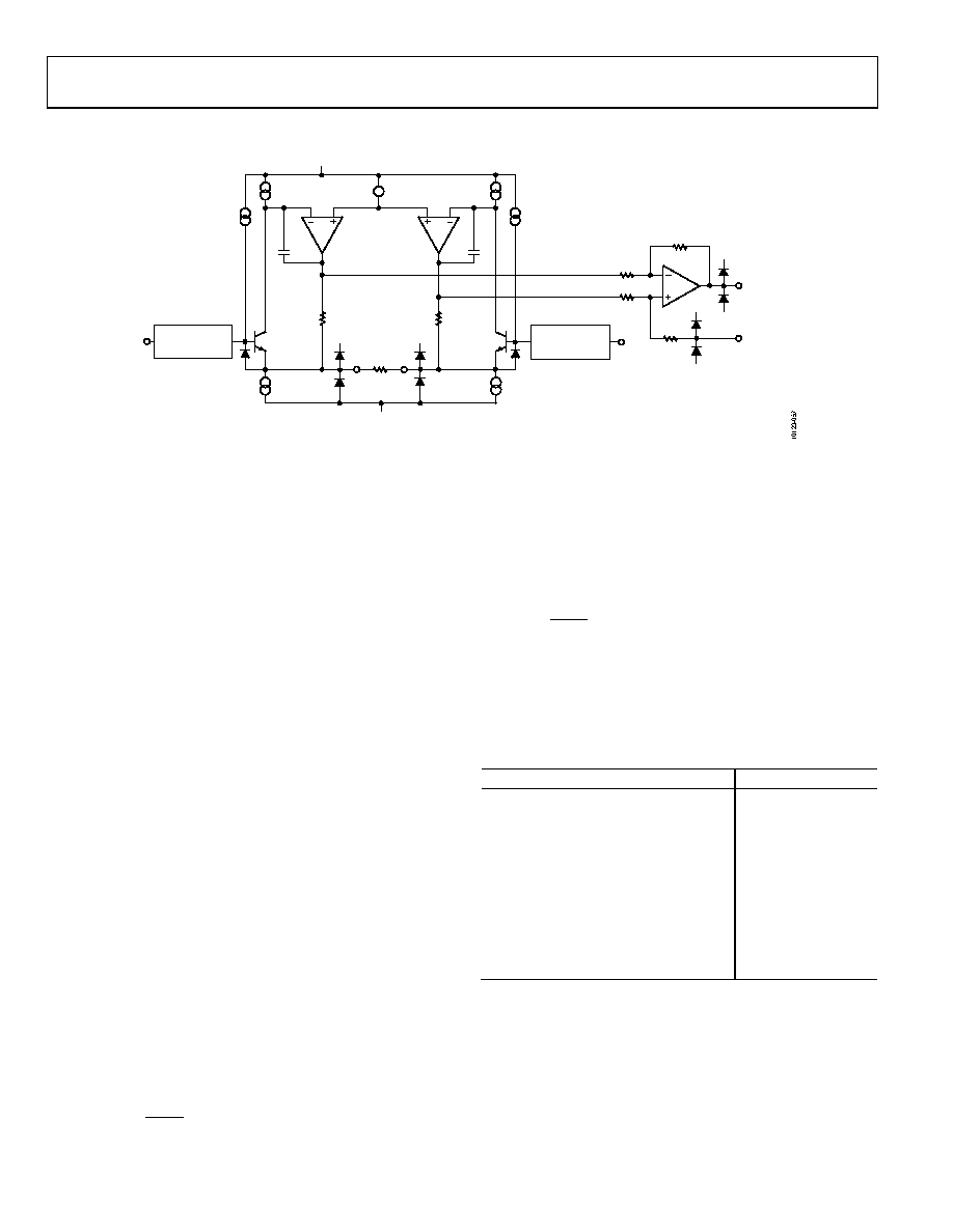 AD8421 Data Sheet Rev. 0 | Page 20 of 28 THEORY OF OPERATION A3 A1 A2 Q2 Q1 C1 C2 +IN –IN +VS –VS 10kΩ 10kΩ 10kΩ +VS –VS OUTPUT REF NODE 1 NODE 2 IB COMPENSATION IB COMPENSATION RG VB II +VS +VS +VS 10kΩ R1 4.95kΩ R2 4.95kΩ DIFFERENCE AMPLIFIER STAGE GAIN STAGE I I ESD AND OVERVOLTAGE PROTECTION ESD AND OVERVOLTAGE PROTECTION superβ NODE 3 NODE 4 superβ –VS Figure 61. Simplified Schematic ARCHITECTURE The AD8421 is based on the classic 3-op-amp topology. This topology has two stages: a preamplifier to provide differential amplification, followed by a difference amplifier that removes the common-mode voltage. Figure 61 shows a simplified schematic of the AD8421. Topologically, Q1, A1, R1 and Q2, A2, R2 can be viewed as precision current feedback amplifiers. Input Transistors Q1 and Q2 are biased at a fixed current so that any input signal forces the output voltages of A1 and A2 to change accordingly. The differential signal applied to the inputs is replicated across the RG pins. Any current through RG also flows through R1 and R2, creating a gained differential voltage between Node 1 and Node 2. The amplified differential and common-mode signals are applied to a difference amplifier that rejects the common-mode voltage but preserves the amplified differential voltage. The difference amplifier employs innovations that result in very low output errors such as offset voltage and drift, distortion at various loads, as well as output noise. Laser-trimmed resistors allow for a highly accurate in-amp with gain error less than 0.01% and CMRR that exceeds 94 dB (G = 1). The high performance pinout and special attention given to design and layout allow for high CMRR performance across a wide frequency and temperature range. Using superbeta input transistors and bias current compensation, the AD8421 offers extremely high input impedance, low bias cur- rent, low offset current, low current noise, and extremely low voltage noise of 3 nV/√Hz. The current-limiting and overvoltage protection scheme allow the input to go 40 V from the opposite rail at all gains without compromising the noise performance. The transfer function of the AD8421 is VOUT = G × (V+IN − V−IN) + VREF where G = 1 + G R kΩ 9 . 9 Users can easily and accurately set the gain using a single standard resistor. GAIN SELECTION Placing a resistor across the RG terminals sets the gain of the AD8421. The gain can be calculated by referring to Table 6 or by using the following gain equation: RG = 1 kΩ 9 . 9 − G The AD8421 defaults to G = 1 when no gain resistor is used. To determine the total gain accuracy of the system, add the tolerance and gain drift of the RG resistor to the specifications of the AD8421. When the gain resistor is not used, gain error and gain drift are minimal. Table 6. Gains Achieved Using 1% Resistors 1% Standard Table Value of RG Calculated Gain 10 kΩ 1.99 2.49 kΩ 4.98 1.1 kΩ 10.00 523 Ω 19.93 200 Ω 50.50 100 Ω 100.0 49.9 Ω 199.4 20 Ω 496.0 10 Ω 991.0 4.99 Ω 1985 RG Power Dissipation The AD8421 duplicates the differential voltage across its inputs onto the RG resistor. Choose an RG resistor size that is sufficient to handle the expected power dissipation at ambient temperature. |
|
Link URL |
| Does ALLDATASHEET help your business so far? [ DONATE ] |
About Alldatasheet | Advertisement | Contact us | Privacy Policy | Link to Datasheet | Link Exchange | Manufacturer List All Rights Reserved©Alldatasheet.com |
| Russian : Alldatasheetru.com | Korean : Alldatasheet.co.kr | Spanish : Alldatasheet.es | French : Alldatasheet.fr | Italian : Alldatasheetit.com Portuguese : Alldatasheetpt.com | Polish : Alldatasheet.pl | Vietnamese : Alldatasheet.vn Indian : Alldatasheet.in | Mexican : Alldatasheet.com.mx | British : Alldatasheet.co.uk | New Zealand : Alldatasheet.co.nz |
|
Family Site : ic2ic.com |
icmetro.com |
 Indian ▼
 English
 Chinese
 German
 Japanese
 Russian
 Korean
 Spanish
 French
 Italian
 Portuguese
 Polish
 Vietnamese
 Indian
 Mexican
 British
 New Zealand


