 |
Electronic Components Datasheet Search |
|
|
Electronic Components Datasheet Search |
|
The question interval is too short.
Please try again in a few seconds.

Hello, Please ask a question about RF2369 Datasheet
# Example questions:
➢ What are the two different modes the select pin controls, and what voltage levels distinguish between them?
➢ How does increasing the supply voltage (vcc) generally affect the total current consumption (icc) in high gain mode for the cellular lna?
➢ What are the two primary functions of pin 1 (vref/pd) on the device, and how does its functionality differ depending on the application?
| Part No. | RF2369 |
| Manufacturer | RFMD |
| Size | 306 Kbytes |
| Pages | 10 pages |
| Description | 3V LOW NOISE AMPLIFIER/ 3V PA DRIVER AMPLIFIER |

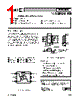




1. Device Overview:
️· Part Number: RFPA0042
️· Function: This is a versatile RF component that can operate as either a Low Noise Amplifier (LNA) or a Driver Amplifier. The selection is controlled by the "SELECT" pin.
️· Frequency Range: Optimized for cellular applications, specifically around 800-900 MHz and 880 MHz ranges are repeatedly mentioned.
️· Applications: Cellular base stations, mobile handsets, and other wireless communication systems.
️· Key Features:
- Low Noise Figure (when configured as an LNA)
- Adjustable bias current via VREF/PD pin.
- Selectable modes (LNA or Driver Amplifier)
- Optimized for low voltage operation (3V).
- Good linearity.
2. Pinout and Functionality:
️· Pin 1 (VREF/PD): Used for bias control. It allows external adjustment of the LNA bias current, giving the user a way to optimize for noise or linearity.
️· Pin 2 (GND1): Ground connection. Important for good performance.
️· Pin 3 (RF IN): RF input pin.
️· Pin 4 (RF OUT): RF output pin. Requires external bias/matching components.
️· Pin 5 (GND2): Ground for emittance inductance.
️· Pin 6 (SELECT): Controls the operating mode.
- SELECT < 1.8V: High Gain (LNA) Mode
- SELECT > 1.8V: Low Gain / Bypass Mode (Driver Amplifier)
3. Performance Characteristics (Key Specs – from graphs & descriptions)
️· Noise Figure (LNA Mode): Relatively low, but exact value varies with voltage and temperature.
️· Gain (LNA Mode): Around 14-17 dB (depending on Vcc and Temperature).
️· Gain (Driver Mode): Much lower gain in bypass mode.
️· IIP3 (Third-Order Intercept Point): Indicates linearity. Values around 20-29 dBm. This varies depending on the mode and Vcc
️· S11 & S22: The graphs depict the input and output matching characteristics (reflection coefficient) in both LNA and Bypass modes.
️· Current Consumption: The total DC current (Icc) varies depending on the mode and supply voltage.
️· Voltage: Optimized for 3V operation.
️· Temperature: Performance parameters are shown across a temperature range (-30C to 85C).
4. Application Information:
️· Application Schematics: Provides example circuit configurations for:
- Cellular LNA (~881MHz)
- Cellular Driver Amplifier (~836MHz)
️· Evaluation Board: Describes an evaluation board layout and schematic, which is helpful for testing and prototyping.
️· Bias Control: Emphasizes the importance of the VREF/PD pin for adjusting the bias current and optimizing performance.
️· Matching Networks: Suggests external matching networks are required on the RF IN and RF OUT.
5. Key Graphs & Data:
️· Noise Figure vs. Vcc (LNA): Illustrates how the noise figure changes with supply voltage.
️· Gain vs. Vcc (LNA & Bypass): Shows how gain varies with supply voltage in both modes.
️· IIP3 vs. Vcc (LNA & Bypass): Indicates the linearity performance with different supply voltages.
️· S-Parameter plots: Shows how well the device is matched to 50 Ohms.
Important Considerations:
️· External Matching: The device *requires* external matching networks to achieve optimal performance. The datasheet shows some example circuits.
️· Bias Adjustment: The VREF/PD pin is critical for tuning the device for specific performance requirements (noise vs. linearity).
️· Supply Voltage: The device is designed for 3V operation.
1. Device Overview:
️· Part Number: RFPA0042
️· Function: This is a versatile RF component that can operate as either a Low Noise Amplifier (LNA) or a Driver Amplifier. The selection is controlled by the "SELECT" pin.
️· Frequency Range: Optimized for cellular applications, specifically around 800-900 MHz and 880 MHz ranges are repeatedly mentioned.
️· Applications: Cellular base stations, mobile handsets, and other wireless communication systems.
️· Key Features:
- Low Noise Figure (when configured as an LNA)
- Adjustable bias current via VREF/PD pin.
- Selectable modes (LNA or Driver Amplifier)
- Optimized for low voltage operation (3V).
- Good linearity.
2. Pinout and Functionality:
️· Pin 1 (VREF/PD): Used for bias control. It allows external adjustment of the LNA bias current, giving the user a way to optimize for noise or linearity.
️· Pin 2 (GND1): Ground connection. Important for good performance.
️· Pin 3 (RF IN): RF input pin.
️· Pin 4 (RF OUT): RF output pin. Requires external bias/matching components.
️· Pin 5 (GND2): Ground for emittance inductance.
️· Pin 6 (SELECT): Controls the operating mode.
- SELECT < 1.8V: High Gain (LNA) Mode
- SELECT > 1.8V: Low Gain / Bypass Mode (Driver Amplifier)
3. Performance Characteristics (Key Specs – from graphs & descriptions)
️· Noise Figure (LNA Mode): Relatively low, but exact value varies with voltage and temperature.
️· Gain (LNA Mode): Around 14-17 dB (depending on Vcc and Temperature).
️· Gain (Driver Mode): Much lower gain in bypass mode.
️· IIP3 (Third-Order Intercept Point): Indicates linearity. Values around 20-29 dBm. This varies depending on the mode and Vcc
️· S11 & S22: The graphs depict the input and output matching characteristics (reflection coefficient) in both LNA and Bypass modes.
️· Current Consumption: The total DC current (Icc) varies depending on the mode and supply voltage.
️· Voltage: Optimized for 3V operation.
️· Temperature: Performance parameters are shown across a temperature range (-30C to 85C).
4. Application Information:
️· Application Schematics: Provides example circuit configurations for:
- Cellular LNA (~881MHz)
- Cellular Driver Amplifier (~836MHz)
️· Evaluation Board: Describes an evaluation board layout and schematic, which is helpful for testing and prototyping.
️· Bias Control: Emphasizes the importance of the VREF/PD pin for adjusting the bias current and optimizing performance.
️· Matching Networks: Suggests external matching networks are required on the RF IN and RF OUT.
5. Key Graphs & Data:
️· Noise Figure vs. Vcc (LNA): Illustrates how the noise figure changes with supply voltage.
️· Gain vs. Vcc (LNA & Bypass): Shows how gain varies with supply voltage in both modes.
️· IIP3 vs. Vcc (LNA & Bypass): Indicates the linearity performance with different supply voltages.
️· S-Parameter plots: Shows how well the device is matched to 50 Ohms.
Important Considerations:
️· External Matching: The device *requires* external matching networks to achieve optimal performance. The datasheet shows some example circuits.
️· Bias Adjustment: The VREF/PD pin is critical for tuning the device for specific performance requirements (noise vs. linearity).
️· Supply Voltage: The device is designed for 3V operation.
| Part No. | RF2369 |
| Manufacturer | RFMD |
| Size | 306 Kbytes |
| Pages | 10 pages |
| Description | 3V LOW NOISE AMPLIFIER/ 3V PA DRIVER AMPLIFIER |
| Does ALLDATASHEET help your business so far? [ DONATE ] |
About Alldatasheet | Advertisement | Contact us | Privacy Policy | Link to Datasheet | Link Exchange | Manufacturer List All Rights Reserved©Alldatasheet.com |
| Russian : Alldatasheetru.com | Korean : Alldatasheet.co.kr | Spanish : Alldatasheet.es | French : Alldatasheet.fr | Italian : Alldatasheetit.com Portuguese : Alldatasheetpt.com | Polish : Alldatasheet.pl | Vietnamese : Alldatasheet.vn Indian : Alldatasheet.in | Mexican : Alldatasheet.com.mx | British : Alldatasheet.co.uk | New Zealand : Alldatasheet.co.nz |
|
Family Site : ic2ic.com |
icmetro.com |
 Indian ▼
  English
 Chinese
 German
 Japanese
 Russian
 Korean
 Spanish
 French
 Italian
 Portuguese
 Polish
 Vietnamese
 Mexican
 British
 New Zealand