4-401
Product Description
Ordering Information
Typical Applications
Features
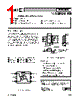
Functional Block Diagram
RF Micro Devices, Inc.
7628 Thorndike Road
Greensboro, NC 27409, USA
Tel (336) 664 1233
Fax (336) 664 0454
http://www.rfmd.com
Optimum Technology Matching® Applied
Si BJT
GaAs MESFET
GaAs HBT
Si Bi-CMOS
SiGe HBT
Si CMOS
InGaP/HBT
GaN HEMT
SiGe Bi-CMOS
2
GND1
3
RF IN
4
RF OUT
5
GND2
Logic
Control
1
VREF/PD
SELECT
6
RF2369
3V LOW NOISE AMPLIFIER/
3V PA DRIVER AMPLIFIER
• CDMA/Cellular Bypass LNA
• CDMA/Cellular Bypass Driver Amplifier
• General Purpose Amplification
• Commercial and Consumer Systems
The RF2369 is a switchable low noise amplifier with a
very high dynamic range designed for digital cellular
applications. The device functions as an outstanding front
end low noise amplifier. When used as an LNA, the bias
current can be set externally. When used as a PA driver,
the IC can operate directly from a single cell Li-ion battery
and includes a power down feature that can be used to
completely turn off the device. The IC is featured in a
standard SOT 6-lead plastic package.
• Low Noise and High Intercept Point
• Adjustable Bias Current
• LNA Bypass Loss is +2dB
• 150MHz to 2500MHz Operation
• Meets IMD Tests with Two Gain
States/Single Logic Control Line
RF2369
3V Low Noise Amplifier/ 3V PA Driver Amplifier
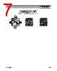
RF2369PCBA-41X Fully Assembled Evaluation Board (LNA)
0
Rev B2 061016
0.10
MAX.
0.90
0.70
1.30
1.00
1.90
3.10
2.70
0.50
0.35
3.00
2.60
1.80
1.40
9°
1°
0.25
0.10
0.37 MIN.
Shaded lead is pin 1.
Dimensions in mm.
*When Pin 1 is in upper left,
text reads downward
(as shown).
Package Style: SOT 6-Lead
RoHS Compliant & Pb-Free Product

 Indian ▼
 English
 Chinese
 German
 Japanese
 Russian
 Korean
 Spanish
 French
 Italian
 Portuguese
 Polish
 Vietnamese
 Indian
 Mexican
 British
 New Zealand