 |
Electronic Components Datasheet Search |
|
|
Electronic Components Datasheet Search |
|
The question interval is too short.
Please try again in a few seconds.

Hello, Please ask a question about DMC3025LSD Datasheet
# Example questions:
➢ What is the typical on-resistance (rds(on)) value when vgs = 4.5v and id = 5a?
➢ How does on-resistance change with increasing junction temperature?
➢ What is the relationship between total gate charge (qg) and the drain-source voltage (vds)?
| Part No. | DMC3025LSD |
| Manufacturer | DIODES |
| Size | 350 Kbytes |
| Pages | 10 pages |
| Description | 30V COMPLEMENTARY ENHANCEMENT MODE MOSFET |

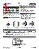
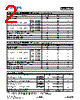
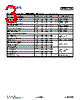
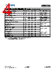
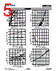
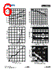
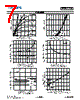
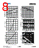

1. General Description
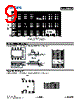
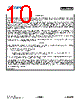
️· It's a power MOSFET (Metal-Oxide-Semiconductor Field-Effect Transistor). Likely used in switching applications.
2. Key Electrical Characteristics (Typical Values at Ta = 25°C unless otherwise noted)
️· Vds (Drain-Source Voltage): Rated for a significant voltage (see Maximum Ratings below)
️· Ids (Drain Current): Capable of handling substantial drain current.
️· Rds(on) (Drain-Source On-Resistance): Relatively low on-resistance which reduces power losses during switching.
️· Qg (Total Gate Charge): Indicates the amount of charge required to turn the MOSFET on. This impacts gate drive requirements.
️· Ciss, Coss, Crss (Input, Output, and Reverse Transfer Capacitance): These capacitance values relate to switching speed and power dissipation. Lower values generally mean faster switching.
3. Maximum Ratings
️· Vds (Drain-Source Voltage): A high voltage, indicating suitability for higher-voltage applications.
️· Id (Drain Current): The maximum continuous current the MOSFET can handle.
️· Pd (Power Dissipation): Maximum power the MOSFET can dissipate without overheating. Limited by both heat sink and junction temperature.
️· Junction Temperature (Tj): The maximum allowed temperature of the silicon die. Exceeding this can lead to device failure.
️· Storage Temperature: Range of temperature the device can be stored at.
️· Tj(max) (Maximum Junction Temperature): 150°C – *A critical parameter. Ensure your application keeps the junction temperature well below this.*
4. Electrical Characteristics (Table Values)
| Parameter | Symbol | Test Conditions | Value(s) | Unit |
|---|---|---|---|---|
| Vds (Max) | Vds | V | ||
| Ids (Max) | Ids | A | ||
| Rds(on) | Rds(on) | Vgs = 10V, Id = 5A | Ω | |
| Qg (Total Gate Charge) | Qg | Vgs = 10V, Vds = 5V, Id = 5A | nC | |
| Ciss, Coss, Crss | Vgs = 10V, Vds = 5V | pF | ||
| Vsd (Source Drain Voltage) |
1. General Description
️· It's a power MOSFET (Metal-Oxide-Semiconductor Field-Effect Transistor). Likely used in switching applications.
2. Key Electrical Characteristics (Typical Values at Ta = 25°C unless otherwise noted)
️· Vds (Drain-Source Voltage): Rated for a significant voltage (see Maximum Ratings below)
️· Ids (Drain Current): Capable of handling substantial drain current.
️· Rds(on) (Drain-Source On-Resistance): Relatively low on-resistance which reduces power losses during switching.
️· Qg (Total Gate Charge): Indicates the amount of charge required to turn the MOSFET on. This impacts gate drive requirements.
️· Ciss, Coss, Crss (Input, Output, and Reverse Transfer Capacitance): These capacitance values relate to switching speed and power dissipation. Lower values generally mean faster switching.
3. Maximum Ratings
️· Vds (Drain-Source Voltage): A high voltage, indicating suitability for higher-voltage applications.
️· Id (Drain Current): The maximum continuous current the MOSFET can handle.
️· Pd (Power Dissipation): Maximum power the MOSFET can dissipate without overheating. Limited by both heat sink and junction temperature.
️· Junction Temperature (Tj): The maximum allowed temperature of the silicon die. Exceeding this can lead to device failure.
️· Storage Temperature: Range of temperature the device can be stored at.
️· Tj(max) (Maximum Junction Temperature): 150°C – *A critical parameter. Ensure your application keeps the junction temperature well below this.*
4. Electrical Characteristics (Table Values)
| Parameter | Symbol | Test Conditions | Value(s) | Unit |
|---|---|---|---|---|
| Vds (Max) | Vds | V | ||
| Ids (Max) | Ids | A | ||
| Rds(on) | Rds(on) | Vgs = 10V, Id = 5A | Ω | |
| Qg (Total Gate Charge) | Qg | Vgs = 10V, Vds = 5V, Id = 5A | nC | |
| Ciss, Coss, Crss | Vgs = 10V, Vds = 5V | pF | ||
| Vsd (Source Drain Voltage) |
| Part No. | DMC3025LSD |
| Manufacturer | DIODES |
| Size | 350 Kbytes |
| Pages | 10 pages |
| Description | 30V COMPLEMENTARY ENHANCEMENT MODE MOSFET |
| Does ALLDATASHEET help your business so far? [ DONATE ] |
About Alldatasheet | Advertisement | Contact us | Privacy Policy | Link to Datasheet | Link Exchange | Manufacturer List All Rights Reserved©Alldatasheet.com |
| Russian : Alldatasheetru.com | Korean : Alldatasheet.co.kr | Spanish : Alldatasheet.es | French : Alldatasheet.fr | Italian : Alldatasheetit.com Portuguese : Alldatasheetpt.com | Polish : Alldatasheet.pl | Vietnamese : Alldatasheet.vn Indian : Alldatasheet.in | Mexican : Alldatasheet.com.mx | British : Alldatasheet.co.uk | New Zealand : Alldatasheet.co.nz |
|
Family Site : ic2ic.com |
icmetro.com |
 Indian ▼
  English
 Chinese
 German
 Japanese
 Russian
 Korean
 Spanish
 French
 Italian
 Portuguese
 Polish
 Vietnamese
 Mexican
 British
 New Zealand