|
Electronic Components Datasheet Search |
|
|
Electronic Components Datasheet Search |
|
NE5900 Datasheet(PDF) 4 Page - NXP Semiconductors |
|
|
|||||||||||||||||||||||||||||
NE5900 Datasheet(HTML) 4 Page - NXP Semiconductors |
|
|
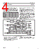
4 / 7 page  Philips Semiconductors Product specification NE5900 Call progress decoder 1986 May 8 4 At the start of an in-band tone (envelope output goes high), a 2.3 second interval is timed out. Transitions of the envelope during this interval are counted to determine the signal present. At 2.3 seconds, the three bits of data representing this decision are stored in the latch and appear at the outputs. A data valid signal goes high at this time, signaling that the data bits, Pins 10 – 12, can be read. The output code is as follows: Pin 12 Pin 11 Pin 10 Dial Tone 0 0 0 Ringing Signal 1 0 0 Busy Signal 0 1 0 Re-order Tone 0 0 1 Overflow 1 1 1 The overflow condition occurs in the event that too many transitions occur during the 2.3 second interval. This can result from noise, voice, or other line disturbances not normally present during the post-dialing interval. Note that the end of dial tone in interpreted as a valid ringing signal. The clear input resets all internal registers and the output latch, and is to be set low after the completion of dialing. The clear input should be pulsed high for proper operation. Recommended pulse width is between 0.2 µs and 20ms. If clear is held high when envelope is high, a false output pulse (Pin 13) can result when clear is returned low. For applications where dialing is done by a person rather than by a microprocessor, an uncertainty exists about the number of digits to be dialed (local vs long distance). In such situations it is possible to clear the NE5900 by application of the DTMF signal or dial pulses to the clear pin (Pin 6). When dialing is complete, the device is cleared and ready to respond to the next call progress unit. Enable is held at 5V to enable Pins 10, 11, 12 and 13. When enable is brought low, data valid is also set low. Enable must remain high while the data is also set low. Enable must remain high while the data is being read. The test pin is for production test only and must be kept low in all user applications. INPUT 10k Ω FILTER ANTI-ALIAS OSCILLATOR 3.58MHz FILTER SC BANDPASS LOGIC DECODER LATCHES DECODER DETECTOR ANALOG BUFFERS TRI-STATE BUFFER DIVIDERS CLOCK R1 R2 10k Ω VREF 5V 0V FILTER LOWPASS DETECTOR DIGITAL EXT CLOCK IN/XTAL1 IN/XTAL2 CLEAR IN COUNT IN PROGRESS DATA VALID TRI-STATE ENABLE ENVELOPE BIT 1 BIT 2 BIT 3 TIMER 2.3 SECOND SR01144 Figure 3. Detailed Block Diagram CPD Figure 4 shows a typical application of the call progress decoder. In this application only one external component is needed an no microprocessor activity other than clear is required. Figure 5 shows the recommended direct interface to the telephone line. Bus connection is possible by utilizing tri-state, and internal timing is accomplished with a 3.58MHz crystal. The designer can utilize the input signal, clock, bus, or microprocessor interface which best serves the application. Figure 6 gives a typical timing diagram for the application of Figures 4 and 5. |
|
|
Link URL |
| Does ALLDATASHEET help your business so far? [ DONATE ] |
About Alldatasheet | Advertisement | Contact us | Privacy Policy | Link to Datasheet | Link Exchange | Manufacturer List All Rights Reserved©Alldatasheet.com |
| Russian : Alldatasheetru.com | Korean : Alldatasheet.co.kr | Spanish : Alldatasheet.es | French : Alldatasheet.fr | Italian : Alldatasheetit.com Portuguese : Alldatasheetpt.com | Polish : Alldatasheet.pl | Vietnamese : Alldatasheet.vn Indian : Alldatasheet.in | Mexican : Alldatasheet.com.mx | British : Alldatasheet.co.uk | New Zealand : Alldatasheet.co.nz |
|
Family Site : ic2ic.com |
icmetro.com |
 Indian ▼
 English
 Chinese
 German
 Japanese
 Russian
 Korean
 Spanish
 French
 Italian
 Portuguese
 Polish
 Vietnamese
 Indian
 Mexican
 British
 New Zealand