|
Electronic Components Datasheet Search |
|
|
Electronic Components Datasheet Search |
|
TOP209 Datasheet(PDF) 6 Page - Power Integrations, Inc. |
|
|
|||||||||||||||||||||||||||||
TOP209 Datasheet(HTML) 6 Page - Power Integrations, Inc. |
|
|
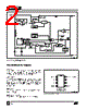
6 / 16 page  A 8/97 6 TOP209/210 2 General Circuit Description Figure 7 shows a low-cost, DC input, flyback switching power supply using the TOP210 integrated circuit. This 5 V, 4 W power supply operates from a DC voltage derived from rectified and filtered AC mains voltage of 85 to 265 VAC. The 5 V output is indirectly sensed via the primary bias winding. The output voltage is determined by the TOPSwitch CONTROL pin shunt regulator voltage (V C), the voltage drops of rectifiers D2 and D3, and the turns ratio between the bias winding and output winding of T1. Other output voltages are also possible by adjusting the transformer turns ratios. The high voltage DC bus is applied to the primary winding of T1. Capacitor C1 filters the high voltage supply, and is only necessary if the connections between the high voltage DC supply and the TOP210 are long. The other side of the transformer primary is driven by the integrated high-voltage MOSFET within the TOP210. D1 and VR1 clamp the voltage spike caused by transformer leakage inductance to a safe value and reduce ringing at the DRAIN of U1. The power secondary winding is rectified and filtered by D2, C2, L1, and C3 to create the 5V output voltage. The bias winding is rectified and filtered by D3, R1 and C5 to create a bias voltage to the TOP210. C5 also filters internal MOSFET gate drive charge current spikes on the CONTROL pin, determines the auto-restart frequency, and together with R1, compensates the control loop. PI-2045-041798 +5 V RTN C1 10 nF 400 V C5 47 µF 10 V D2 1N5822 D3 1N4148 C2 330 µF 10 V T1 D1 UF4005 C3 100 µF 10 V R1 15 Ω VR1 BZY97- C120 120 V L1 3.3 µH CIRCUIT PERFORMANCE: Line Regulation - –1.5% (104-370 VDC) Load Regulation - –5% (10-100%) Ripple Voltage –25 mV + - U1 TOP210 2 1 3 4 5 8 DC INPUT TRD1 D S C CONTROL TOPSwitch Figure 7. Schematic Diagram of a Minimum Parts Count 5 V, 4 W Bias Supply Using the TOP210. |
|
|
Link URL |
| Does ALLDATASHEET help your business so far? [ DONATE ] |
About Alldatasheet | Advertisement | Contact us | Privacy Policy | Link to Datasheet | Link Exchange | Manufacturer List All Rights Reserved©Alldatasheet.com |
| Russian : Alldatasheetru.com | Korean : Alldatasheet.co.kr | Spanish : Alldatasheet.es | French : Alldatasheet.fr | Italian : Alldatasheetit.com Portuguese : Alldatasheetpt.com | Polish : Alldatasheet.pl | Vietnamese : Alldatasheet.vn Indian : Alldatasheet.in | Mexican : Alldatasheet.com.mx | British : Alldatasheet.co.uk | New Zealand : Alldatasheet.co.nz |
|
Family Site : ic2ic.com |
icmetro.com |
 Indian ▼
 English
 Chinese
 German
 Japanese
 Russian
 Korean
 Spanish
 French
 Italian
 Portuguese
 Polish
 Vietnamese
 Indian
 Mexican
 British
 New Zealand