 |
Electronic Components Datasheet Search |
|
|
Electronic Components Datasheet Search |
|
ADP197ACBZ-R7 Datasheet(PDF) 11 Page - Analog Devices |
|
|
|||||||||||||||||||||||||||||
ADP197ACBZ-R7 Datasheet(HTML) 11 Page - Analog Devices |
|
|
11 / 16 page 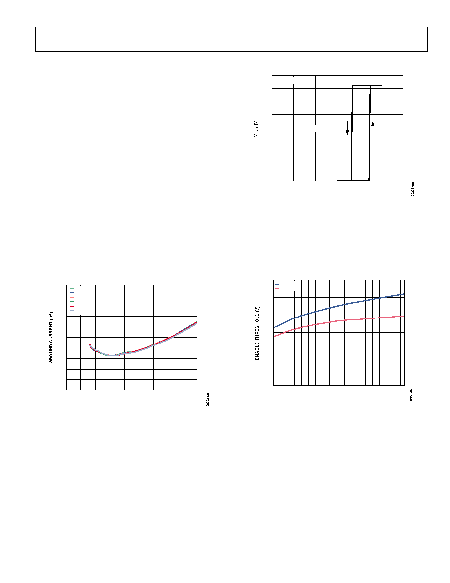 ADP197 Rev. 0 | Page 11 of 16 APPLICATIONS INFORMATION CAPACITOR SELECTION Output Capacitor The ADP197 is designed for operation with small, space-saving ceramic capacitors but functions with most commonly used capa- citors when the effective series resistance (ESR) value is carefully considered. The ESR of the output capacitor affects the response to load transients. A typical 1 μF capacitor with an ESR of 0.1 Ω or less is recommended for good transient response. Using a larger value of output capacitance improves the transient response to large changes in load current. Input Bypass Capacitor Connecting at least 1 μF of capacitance from VIN to GND reduces the circuit sensitivity to the printed circuit board (PCB) layout, especially when high source impedance or long input traces are encountered. When greater than 1 μF of output capacitance is required, increase the input capacitor to match it. GROUND CURRENT The major source for ground current in the ADP197 is the internal charge pump for the FET drive circuitry. Figure 24 shows the typical ground current when VEN = VIN, and varies from 1.8 V to 5.5 V. 0 5 10 15 20 25 30 35 40 45 50 1.0 1.5 2.0 2.5 3.0 3.5 4.0 4.5 5.0 5.5 VIN (V) 50mA 100mA 200mA 500mA 1000mA 3000mA Figure 24. Ground Current vs. Load Current, Different Input Voltages (VIN) ENABLE FEATURE The ADP197 uses the EN pin to enable and disable the VOUT pin under normal operating conditions. As shown in Figure 25, when a rising voltage (VEN) on the EN pin crosses the active threshold, VOUT turns on. When a falling voltage (VEN) on the EN pin crosses the inactive threshold, VOUT turns off. 0 0.5 1.0 1.5 2.0 2.5 3.0 3.5 4.0 0 0.2 0.4 0.6 0.8 1.0 1.2 ENABLE VOLTAGE (V) VEN FALLING VEN RISING VOUT AT 3.6V Figure 25. Typical EN Operation As shown in Figure 25, the EN pin has hysteresis built into it. This prevents on/off oscillations that can occur due to noise on the EN pin as it passes through the threshold points. The EN pin active/inactive thresholds derive from the VIN voltage; therefore, these thresholds vary with the changing input voltage. Figure 26 shows the typical EN active/inactive thresholds when the input voltage varies from 1.8 V to 5.5 V. 0 0.2 0.4 0.6 0.8 1.0 1.2 1.82.22.63.03.43.8 4.24.65.05.4 INPUT VOLTAGE (V) EN RISE EN FALL Figure 26. Typical EN Thresholds vs. Input Voltage (VIN) TIMING Turn-on delay is defined as the interval between the time that VEN exceeds the rising threshold voltage and when VOUT rises to ~10% of its final value. The ADP197 includes circuitry that has a typical 1 ms turn-on delay and a controlled rise time to limit the VIN inrush current. As shown in Figure 27 and Figure 28, the turn- on delay is nearly independent of the input voltage. |
|
|
Link URL |
| Does ALLDATASHEET help your business so far? [ DONATE ] |
About Alldatasheet | Advertisement | Contact us | Privacy Policy | Link to Datasheet | Link Exchange | Manufacturer List All Rights Reserved©Alldatasheet.com |
| Russian : Alldatasheetru.com | Korean : Alldatasheet.co.kr | Spanish : Alldatasheet.es | French : Alldatasheet.fr | Italian : Alldatasheetit.com Portuguese : Alldatasheetpt.com | Polish : Alldatasheet.pl | Vietnamese : Alldatasheet.vn Indian : Alldatasheet.in | Mexican : Alldatasheet.com.mx | British : Alldatasheet.co.uk | New Zealand : Alldatasheet.co.nz |
|
Family Site : ic2ic.com |
icmetro.com |
 Indian ▼
 English
 Chinese
 German
 Japanese
 Russian
 Korean
 Spanish
 French
 Italian
 Portuguese
 Polish
 Vietnamese
 Indian
 Mexican
 British
 New Zealand


