|
Electronic Components Datasheet Search |
|
|
Electronic Components Datasheet Search |
|
M95160-R Datasheet(PDF) 27 Page - STMicroelectronics |
|
|
|||||||||||||||||||||||||||||
M95160-R Datasheet(HTML) 27 Page - STMicroelectronics |
|
|
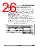
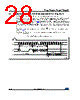
27 / 47 page 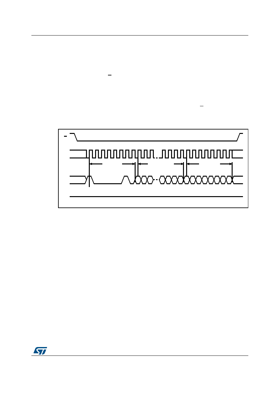 DocID022580 Rev 5 27/47 M95160 M95160-W M95160-R M95160-DF Instructions 46 6.8 Write Identification Page (available only in M95160-D devices) The Write Identification Page (WRID) instruction is used to write the Identification Page (additional page of 32 bytes which can also be permanently locked in Read-only mode). The Chip Select signal (S) is first driven low, and then the bits of the instruction byte, address bytes, and at least one data byte are shifted in (MSB first) on Serial Data input (D). Address bit A10 must be 0, other upper address bits are Don't Care (it might be easier to define these bits as 0, as shown in Table 4). The lower address bits [A4:A0] define the byte address inside the identification page. The self-timed Write cycle starts from the rising edge of Chip Select (S), and continues for a period tW (as specified in Section 9: DC and AC parameters). Figure 16. Write identification page sequence The instruction is discarded, and is not executed, under the following conditions: • If the Write Enable Latch (WEL) bit has not been set to 1 (by executing a Write Enable instruction just before). • If a Write cycle is already in progress. • If the device has not been deselected, by driving high Chip Select (S), at exactly a byte boundary (after the eighth bit, b0, of the last data byte that has been latched in). |
|
Link URL |
| Does ALLDATASHEET help your business so far? [ DONATE ] |
About Alldatasheet | Advertisement | Contact us | Privacy Policy | Link to Datasheet | Link Exchange | Manufacturer List All Rights Reserved©Alldatasheet.com |
| Russian : Alldatasheetru.com | Korean : Alldatasheet.co.kr | Spanish : Alldatasheet.es | French : Alldatasheet.fr | Italian : Alldatasheetit.com Portuguese : Alldatasheetpt.com | Polish : Alldatasheet.pl | Vietnamese : Alldatasheet.vn Indian : Alldatasheet.in | Mexican : Alldatasheet.com.mx | British : Alldatasheet.co.uk | New Zealand : Alldatasheet.co.nz |
|
Family Site : ic2ic.com |
icmetro.com |
 Indian ▼
 English
 Chinese
 German
 Japanese
 Russian
 Korean
 Spanish
 French
 Italian
 Portuguese
 Polish
 Vietnamese
 Indian
 Mexican
 British
 New Zealand