|
Electronic Components Datasheet Search |
|
|
Electronic Components Datasheet Search |
|
MCP1725 Datasheet(PDF) 7 Page - Microchip Technology |
|
|
|||||||||||||||||||||||||||||
MCP1725 Datasheet(HTML) 7 Page - Microchip Technology |
|
|
7 / 32 page 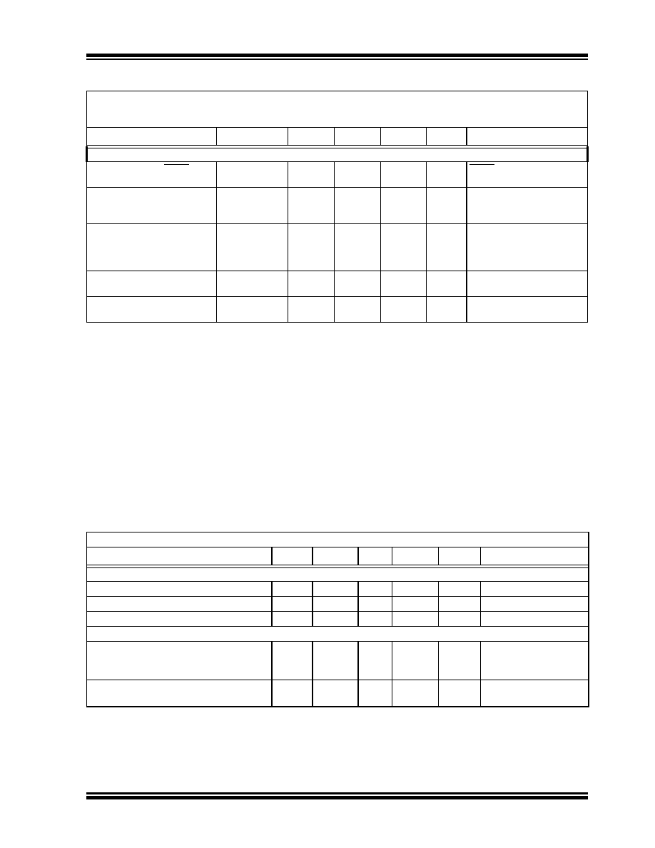 © 2006 Microchip Technology Inc. DS22026A-page 7 MCP1725 TEMPERATURE SPECIFICATIONS AC Performance Output Delay From SHDN TOR — 100 — µs SHDN = GND to VIN VOUT = GND to 95% VR Output Noise eN —2.0 — µV/ √Hz IOUT = 200 mA, f = 1 kHz, COUT = 10 µF (X7R Ceramic), VOUT = 2.5V Power Supply Ripple Rejection Ratio PSRR — 60 — dB f = 100 Hz, COUT = 10 µF, IOUT = 10 mA, VINAC = 30 mV pk-pk, CIN = 0 µF Thermal Shutdown Temperature TSD — 150 — °C IOUT = 100 µA, VOUT = 1.8V, VIN = 2.8V Thermal Shutdown Hysteresis ΔTSD —10 — °C IOUT = 100 µA, VOUT = 1.8V, VIN = 2.8V Electrical Specifications: Unless otherwise indicated, all limits apply for VIN = 2.3V to 6.0V. Parameters Sym Min Typ Max Units Conditions Temperature Ranges Operating Junction Temperature Range TJ -40 — +125 °C Steady State Maximum Junction Temperature TJ — — +150 °C Transient Storage Temperature Range TA -65 — +150 °C Thermal Package Resistances Thermal Resistance, 8LD 2x3 DFN θJA — 52 — °C/W 4-Layer JC51-7 Standard Board with vias Thermal Resistance, 8LD SOIC θJA — 150 — °C/W 4-Layer JC51-7 Standard Board AC/DC CHARACTERISTICS (CONTINUED) Electrical Specifications: Unless otherwise noted, VIN = VOUT(MAX) + VDROPOUT(MAX) (Note 1), VR = 1.8V for Adjustable Output, IOUT = 1 mA, CIN = COUT = 4.7 µF (X7R Ceramic), TA = +25°C. Boldface type applies for junction temperatures, TJ (Note 7) of -40°C to +125°C Parameters Sym Min Typ Max Units Conditions Note 1: The minimum VIN must meet two conditions: VIN ≥ 2.3V and VIN ≥ VOUT(MAX) + VDROPOUT(MAX). 2: VR is the nominal regulator output voltage for the fixed cases. VR = 1.2V, 1.8V, etc. VR is the desired set point output voltage for the adjustable cases. VR = VADJ * ((R1/R2)+1). Figure 4-1. 3: TCVOUT = (VOUT-HIGH – VOUT-LOW) *106 / (VR * ΔTemperature). VOUT-HIGH is the highest voltage measured over the temperature range. VOUT-LOW is the lowest voltage measured over the temperature range. 4: Load regulation is measured at a constant junction temperature using low duty-cycle pulse testing. Load regulation is tested over a load range from 1 mA to the maximum specified output current. 5: Dropout voltage is defined as the input-to-output voltage differential at which the output voltage drops 2% below its nominal value that was measured with an input voltage of VOUT = VR + VDROPOUT(MAX). 6: The maximum allowable power dissipation is a function of ambient temperature, the maximum allowable junction temperature and the thermal resistance from junction to air. (i.e., TA, TJ, θJA). Exceeding the maximum allowable power dissipation will cause the device operating junction temperature to exceed the maximum +150°C rating. Sustained junction temperatures above +150°C can impact device reliability. 7: The junction temperature is approximated by soaking the device under test at an ambient temperature equal to the desired junction temperature. The test time is small enough such that the rise in the junction temperature over the ambient temperature is not significant. |
|
Link URL |
| Does ALLDATASHEET help your business so far? [ DONATE ] |
About Alldatasheet | Advertisement | Contact us | Privacy Policy | Link to Datasheet | Link Exchange | Manufacturer List All Rights Reserved©Alldatasheet.com |
| Russian : Alldatasheetru.com | Korean : Alldatasheet.co.kr | Spanish : Alldatasheet.es | French : Alldatasheet.fr | Italian : Alldatasheetit.com Portuguese : Alldatasheetpt.com | Polish : Alldatasheet.pl | Vietnamese : Alldatasheet.vn Indian : Alldatasheet.in | Mexican : Alldatasheet.com.mx | British : Alldatasheet.co.uk | New Zealand : Alldatasheet.co.nz |
|
Family Site : ic2ic.com |
icmetro.com |
 Indian ▼
 English
 Chinese
 German
 Japanese
 Russian
 Korean
 Spanish
 French
 Italian
 Portuguese
 Polish
 Vietnamese
 Indian
 Mexican
 British
 New Zealand