|
Electronic Components Datasheet Search |
|
|
Electronic Components Datasheet Search |
|
MCP1725 Datasheet(PDF) 17 Page - Microchip Technology |
|
|
|||||||||||||||||||||||||||||
MCP1725 Datasheet(HTML) 17 Page - Microchip Technology |
|
|
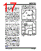
17 / 32 page  © 2006 Microchip Technology Inc. DS22026A-page 17 MCP1725 4.4 Input Capacitor Low input source impedance is necessary for the LDO output to operate properly. When operating from batteries, or in applications with long lead length (> 10 inches) between the input source and the LDO, some input capacitance is recommended. A minimum of 1.0 µF to 4.7 µF is recommended for most applications. For applications that have output step load requirements, the input capacitance of the LDO is very important. The input capacitance provides the LDO with a good local low-impedance source to pull the transient currents from in order to respond quickly to the output load step. For good step response performance, the input capacitor should be of equivalent (or higher) value than the output capacitor. The capacitor should be placed as close to the input of the LDO as is practical. Larger input capacitors will also help reduce any high-frequency noise on the input and output of the LDO and reduce the effects of any inductance that exists between the input source voltage and the input capacitance of the LDO. 4.5 Power Good Output (PWRGD) The PWRGD output is used to indicate when the output voltage of the LDO is within 92% (typical value, see Section 1.0 “Electrical Characteristics” for Minimum and Maximum specifications) of its nominal regulation value. As the output voltage of the LDO rises, the PWRGD output will be held low until the output voltage has exceeded the power good threshold plus the hysteresis value. Once this threshold has been exceeded, the power good time delay is started (shown as TPG in Section 1.0 “Electrical Characteristics”). The power good time delay is adjustable via the CDELAY pin of the LDO (see Section 4.6 “CDELAY Input”). By placing a capacitor from the CDELAY pin to ground, the power good time delay can be adjusted from 200 µs (no capacitance) to 300 ms (0.1 µF capacitor). After the time delay period, the PWRGD output will go high, indicating that the output voltage is stable and within regulation limits. If the output voltage of the LDO falls below the power good threshold, the power good output will transition low. The power good circuitry has a 170 µs delay when detecting a falling output voltage, which helps to increase noise immunity of the power good output and avoid false triggering of the power good output during fast output transients. See Figure 4-2 for power good timing characteristics. When the LDO is put into Shutdown mode using the SHDN input, the power good output is pulled low immediately, indicating that the output voltage will be out of regulation. The timing diagram for the power good output when using the shutdown input is shown in Figure 4-3. The power good output is an open-drain output that can be pulled up to any voltage that is equal to or less than the LDO input voltage. This output is capable of sinking 1.2 mA (VPWRGD < 0.4V maximum). FIGURE 4-2: Power Good Timing. FIGURE 4-3: Power Good Timing from Shutdown. TPG TVDET_PWRGD VPWRGD_TH VOUT PWRGD VOL VOH VIN SHDN VOUT 30 µs 70 µs TOR PWRGD TPG |
|
Link URL |
| Does ALLDATASHEET help your business so far? [ DONATE ] |
About Alldatasheet | Advertisement | Contact us | Privacy Policy | Link to Datasheet | Link Exchange | Manufacturer List All Rights Reserved©Alldatasheet.com |
| Russian : Alldatasheetru.com | Korean : Alldatasheet.co.kr | Spanish : Alldatasheet.es | French : Alldatasheet.fr | Italian : Alldatasheetit.com Portuguese : Alldatasheetpt.com | Polish : Alldatasheet.pl | Vietnamese : Alldatasheet.vn Indian : Alldatasheet.in | Mexican : Alldatasheet.com.mx | British : Alldatasheet.co.uk | New Zealand : Alldatasheet.co.nz |
|
Family Site : ic2ic.com |
icmetro.com |
 Indian ▼
 English
 Chinese
 German
 Japanese
 Russian
 Korean
 Spanish
 French
 Italian
 Portuguese
 Polish
 Vietnamese
 Indian
 Mexican
 British
 New Zealand