|
Electronic Components Datasheet Search |
|
|
Electronic Components Datasheet Search |
|
CLC1605 Datasheet(PDF) 14 Page - Exar Corporation |
|
|
|||||||||||||||||||||||||||||
CLC1605 Datasheet(HTML) 14 Page - Exar Corporation |
|
|
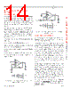
14 / 21 page  Data Sheet ©2007-2013 Exar Corporation 14/21 Rev 1E General Information - Current Feedback Technology Advantages of CFB Technology The CLC1605 Family of amplifiers utilize current feedback (CFB) technology to achieve superior performance. The primary advantage of CFB technology is higher slew rate performance when compared to voltage feedback (VFB) architecture. High slew rate contributes directly to better large signal pulse response, full power bandwidth, and distortion. CFB also alleviates the traditional trade-off between closed loop gain and usable bandwidth that is seen with a VFB amplifier. With CFB, the bandwidth is primarily determined by the value of the feedback resistor, Rf. By using optimum feedback resistor values, the bandwidth of a CFB amplifier remains nearly constant with different gain configurations. When designing with CFB amplifiers always abide by these basic rules: • Use the recommended feedback resistor value • Do not use reactive (capacitors, diodes, inductors, etc.) elements in the direct feedback path • Avoid stray or parasitic capacitance across feedback resistors • Follow general high-speed amplifier layout guidelines • Ensure proper precautions have been made for driving capacitive loads Figure 1. Non-Inverting Gain Configuration with First Order Transfer Function V OUT V IN = − R f R g + 1 Eq. 2 1 + R f Z o(jω) VIN VOUT Zo*Ierr Ierr RL Rf x1 Rg Figure 2. Inverting Gain Configuration with First Order Transfer Function CFB Technology - Theory of Operation Figure 1 shows a simple representation of a current feedback amplifier that is configured in the traditional non-inverting gain configuration. Instead of having two high-impedance inputs similar to a VFB amplifier, the inputs of a CFB amplifier are connected across a unity gain buffer. This buffer has a high impedance input and a low impedance output. It can source or sink current (Ierr) as needed to force the non-inverting input to track the value of Vin. The CFB architecture employs a high gain trans-impedance stage that senses Ierr and drives the output to a value of (Zo(jω) * Ierr) volts. With the application of negative feedback, the amplifier will drive the output to a voltage in a manner which tries to drive Ierr to zero. In practice, primarily due to limitations on the value of Zo(jω), Ierr remains a small but finite value. A closer look at the closed loop transfer function (Eq.1) shows the effect of the trans-impedance, Zo(jω) on the gain of the circuit. At low frequencies where Zo(jω) is very large with respect to Rf, the second term of the equation approaches unity, allowing Rf and Rg to set the gain. At higher frequencies, the value of Zo(jω) will roll off, and the effect of the secondary term will begin to dominate. The -3dB small signal parameter specifies the frequency where the value Zo(jω) equals the value of Rf causing the gain to drop by 0.707 of the value at DC. For more information regarding current feedback amplifiers, visit www.exar.com for detailed application notes, such as AN-3: The Ins and Outs of Current Feedback Amplifiers. V OUT V IN = 1 + R f R g + 1 Eq. 1 1 + R f Z o(jω) VIN VOUT Zo*Ierr Ierr Rg RL Rf x1 |
|
|
Link URL |
| Does ALLDATASHEET help your business so far? [ DONATE ] |
About Alldatasheet | Advertisement | Contact us | Privacy Policy | Link to Datasheet | Link Exchange | Manufacturer List All Rights Reserved©Alldatasheet.com |
| Russian : Alldatasheetru.com | Korean : Alldatasheet.co.kr | Spanish : Alldatasheet.es | French : Alldatasheet.fr | Italian : Alldatasheetit.com Portuguese : Alldatasheetpt.com | Polish : Alldatasheet.pl | Vietnamese : Alldatasheet.vn Indian : Alldatasheet.in | Mexican : Alldatasheet.com.mx | British : Alldatasheet.co.uk | New Zealand : Alldatasheet.co.nz |
|
Family Site : ic2ic.com |
icmetro.com |
 Indian ▼
 English
 Chinese
 German
 Japanese
 Russian
 Korean
 Spanish
 French
 Italian
 Portuguese
 Polish
 Vietnamese
 Indian
 Mexican
 British
 New Zealand