|
Electronic Components Datasheet Search |
|
|
Electronic Components Datasheet Search |
|
DI-57 Datasheet(PDF) 1 Page - Power Integrations, Inc. |
|
|
|||||||||||||||||||||||||||||
DI-57 Datasheet(HTML) 1 Page - Power Integrations, Inc. |
|
|
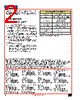
1 / 2 page  U1 DPA426R D2 SBG3045CT D1 BAV19WS C3 1 µF 100 V D4 ES2D VR1 SMCJ 100 A 2 9,10 6,7 NC 4 5 1 C5 220 nF R2 68 Ω 1/4 W C4 180 pF 200 V C6 68 µF 10 V C7 1 nF 1.5 kV R14 10 Ω U2 R15, R16 33 Ω 1/4 W C9 2.2 nF 50 V R3 8.8 kΩ 1% R1 619 kΩ 1% R4 1.0 Ω -VIN L1 1 µH, 2.5 A C23 4.7 µF 20 V C1 1 µF 100 V C2 1 µF 100 V DL SX F C CONTROL CONTROL PI-3662-082603 DPA-Switch T1 RTN 12 V, 5 A U2 PC 357N1T VR2 BTZ52C11 C10-C14 100 µF, 16 V (OSCON) C19 1 µF 16 V C15-C18 47 µF, 16 V (CERAMIC) R7 1 kΩ C8 1 µF 16 V R6 150 Ω + VIN 36-75 VDC www.powerint.com Design Idea DI-57 DPA-Switch 60 W DC-DC Converter August 2003 DI-57 Application Telecom DPA426R 12 V Power Output 60 W Input Voltage Output Voltage Topology Device 36-75 VDC Flyback Figure 1. DPA426R - 60 W, 12 V, 5 A DC-DC Converter. ® ™ Design Highlights • Low cost 400 kHz flyback design • Simple Zener referenced 12 V output • Efficiency – 82% at 36 VDC and full load • Low component count • Accurate line OV and UV protection • Thermal, short circuit and output overload protection • No current sense components Operation DPA-Switch greatly simplifies the design compared to a discrete implementation. Resistor R1 programs the under/over voltages and linearly reduces the maximum duty cycle with input voltage to prevent core saturation during load transients. Resistor R3 programs the DPA-Switch current limit at 85% of nominal to minimize fault and overload power. Drain voltage clamping is provided by diode D4 and Zener diode VR1 with optional components C4 and R2 to provide high frequency snubbing. The output is rectified by diode D2 with optional high frequency damping from components C9, R15 and R16. The output capacitors are alternated to share the ripple current evenly between the Oscon capacitors (C10-14) and the ceramic capacitors (C15-C18). A final decoupling ceramic capacitor C19 is placed at the output pins of the power supply. Output regulation is taken from the +12 V output. Zener diode VR2 is DC-biased by resistor R7 with the opto-diode of U2 providing feedback and resistor R6 programming the gain. Optional capacitor C8 implements a soft-finish network to slow the rise of the output voltage at start-up. |
Similar Part No. - DI-57 |
|
Similar Description - DI-57 |
|
|
|
Link URL |
| Does ALLDATASHEET help your business so far? [ DONATE ] |
About Alldatasheet | Advertisement | Contact us | Privacy Policy | Link to Datasheet | Link Exchange | Manufacturer List All Rights Reserved©Alldatasheet.com |
| Russian : Alldatasheetru.com | Korean : Alldatasheet.co.kr | Spanish : Alldatasheet.es | French : Alldatasheet.fr | Italian : Alldatasheetit.com Portuguese : Alldatasheetpt.com | Polish : Alldatasheet.pl | Vietnamese : Alldatasheet.vn Indian : Alldatasheet.in | Mexican : Alldatasheet.com.mx | British : Alldatasheet.co.uk | New Zealand : Alldatasheet.co.nz |
|
Family Site : ic2ic.com |
icmetro.com |
 Indian ▼
 English
 Chinese
 German
 Japanese
 Russian
 Korean
 Spanish
 French
 Italian
 Portuguese
 Polish
 Vietnamese
 Indian
 Mexican
 British
 New Zealand