 |
Electronic Components Datasheet Search |
|
|
Electronic Components Datasheet Search |
|
STPAC01F2 Datasheet(PDF) 5 Page - STMicroelectronics |
|
|
|||||||||||||||||||||||||||||
STPAC01F2 Datasheet(HTML) 5 Page - STMicroelectronics |
|
|
5 / 7 page 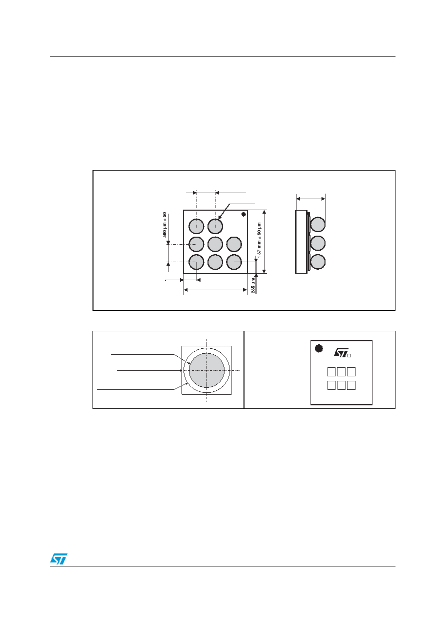 STPAC01F2 Package information 5/7 3 Package information In order to meet environmental requirements, ST offers these devices in ECOPACK® packages. These packages have a lead-free second level interconnect. The category of second level interconnect is marked on the inner box label, in compliance with JEDEC Standard JESD97. The maximum ratings related to soldering conditions are also marked on the inner box label. ECOPACK is an ST trademark. ECOPACK specifications are available at www.st.com. Figure 11. Flip Chip dimensions Figure 12. Footprint Figure 13. Marking 1.57 mm ± 50 µm 315 µm ± 50 500 µm ± 50 650 µm ± 65 285 µm Copper pad Diameter: 250 µm recommended, 300 µm max Solder stencil opening: 330 µm Solder mask opening recommendation: 340 µm min for 300 µm copper pad diameter x y x w z w E Dot, ST logo xx = marking z = manufacturing location yww = datecode (y = year ww = week) |
|
|
Link URL |
| Does ALLDATASHEET help your business so far? [ DONATE ] |
About Alldatasheet | Advertisement | Contact us | Privacy Policy | Link to Datasheet | Link Exchange | Manufacturer List All Rights Reserved©Alldatasheet.com |
| Russian : Alldatasheetru.com | Korean : Alldatasheet.co.kr | Spanish : Alldatasheet.es | French : Alldatasheet.fr | Italian : Alldatasheetit.com Portuguese : Alldatasheetpt.com | Polish : Alldatasheet.pl | Vietnamese : Alldatasheet.vn Indian : Alldatasheet.in | Mexican : Alldatasheet.com.mx | British : Alldatasheet.co.uk | New Zealand : Alldatasheet.co.nz |
|
Family Site : ic2ic.com |
icmetro.com |
 Indian ▼
 English
 Chinese
 German
 Japanese
 Russian
 Korean
 Spanish
 French
 Italian
 Portuguese
 Polish
 Vietnamese
 Indian
 Mexican
 British
 New Zealand


