 |
Electronic Components Datasheet Search |
|
|
Electronic Components Datasheet Search |
|
H8S/2426 Datasheet(PDF) 607 Page - Renesas Technology Corp |
|
|
|||||||||||||||||||||||||||||
H8S/2426 Datasheet(HTML) 607 Page - Renesas Technology Corp |
|
|
607 / 1302 page 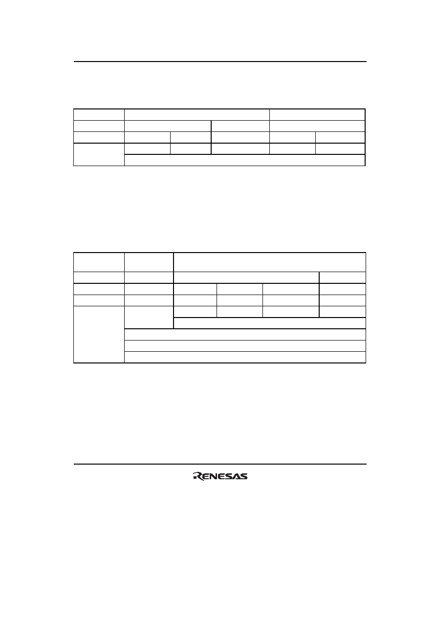 Section 10 I/O Ports Rev. 1.00 Sep. 19, 2008 Page 579 of 1270 REJ09B0466-0100 • P82/IRQ2-B/ETEND2 The pin function is switched as shown below according to the combination of bit ETENDE in EDMDR_2 of the EXDMAC, bit P82DDR, and bit ITS2 in ITSR of the interrupt controller. Operating mode 1, 2, 4, 7 (EXPE = 1) 7 (EXPE = 0) ETENDE 0 1 P82DDR 0 1 0 1 P82 input P82 output ETEND2 output P82 input P82 output Pin function IRQ2-B interrupt input* Note: * IRQ2-B input when the ITS2 bit in ITSR is 1. • P81/EDREQ3/IRQ1-B/TxD3/PO1-B/TIOCB3-B/TMRI1-B The pin function is switched as shown below according to the combination of bit TE in SCR_3 of the SCI, TPU channel 3 settings (by bits MD3 to MD0 in TMDR_3, bits IOB3 to IOB0 in TIORH_3, and bits CCLR2 to CCLR0 in TCR_3), bit NDER1 in NDERL of the PPG, bits PPGS, TPUS, and TMRS in PFCR3, bit P81DDR, and bit ITS1 in ITSR of the interrupt controller. TPU channel 3 settings (1) in table below (2) in table below TE 0 1 P81DDR 0 1 1 NDER1 0 1 P81 input P81 output PO1-B output* 2 TxD3 output TIOCB3-B output* 3 TIOCB3-B input* 3 EDREQ3 input IRQ1-B interrupt input*1 Pin function TMRI1-B input* 4 Notes: 1. IRQ1-B input when the ITS1 bit in ITSR is 1. 2. PO1-B output when the PPGS bit in PFCR3 is 1. 3. TIOCB3-B input/output when the TPUS bit in PFCR3 is 1. 4. TMRI1-B input when the TMRS bit in PFCR3 is 1. |
|
Link URL |
| Does ALLDATASHEET help your business so far? [ DONATE ] |
About Alldatasheet | Advertisement | Contact us | Privacy Policy | Link to Datasheet | Link Exchange | Manufacturer List All Rights Reserved©Alldatasheet.com |
| Russian : Alldatasheetru.com | Korean : Alldatasheet.co.kr | Spanish : Alldatasheet.es | French : Alldatasheet.fr | Italian : Alldatasheetit.com Portuguese : Alldatasheetpt.com | Polish : Alldatasheet.pl | Vietnamese : Alldatasheet.vn Indian : Alldatasheet.in | Mexican : Alldatasheet.com.mx | British : Alldatasheet.co.uk | New Zealand : Alldatasheet.co.nz |
|
Family Site : ic2ic.com |
icmetro.com |
 Indian ▼
 English
 Chinese
 German
 Japanese
 Russian
 Korean
 Spanish
 French
 Italian
 Portuguese
 Polish
 Vietnamese
 Indian
 Mexican
 British
 New Zealand


