 |
Electronic Components Datasheet Search |
|
|
Electronic Components Datasheet Search |
|
DS8113-RNG+ Datasheet(PDF) 7 Page - Maxim Integrated Products |
|
|
|||||||||||||||||||||||||||||
DS8113-RNG+ Datasheet(HTML) 7 Page - Maxim Integrated Products |
|
|
7 / 17 page 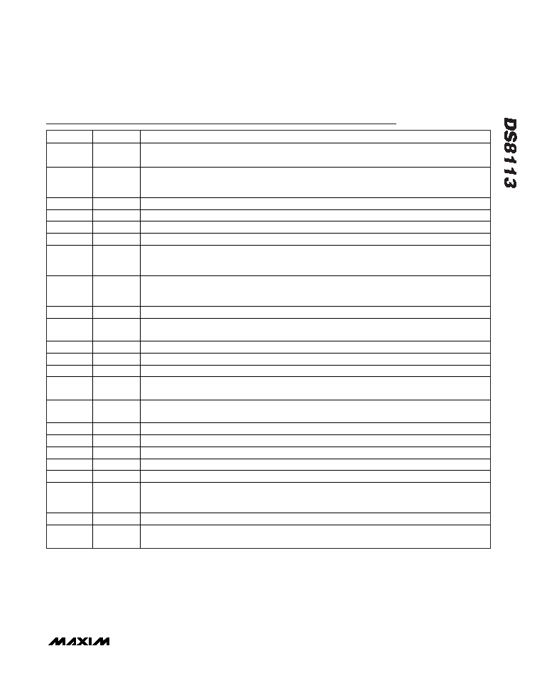 Smart Card Interface _______________________________________________________________________________________ 7 Pin Description PIN NAME FUNCTION 1, 2 CLKDIV1, CLKDIV2 Clock Divider. Determines the divided-down input clock frequency (presented at XTAL1 or from a crystal at XTAL1 and XTAL2) on the CLK output pin. Dividers of 1, 2, 4, and 8 are available. 3 5V/3V 5V/3V Selection Pin. Allows selection of 5V or 3V for communication with an IC card. Logic-high selects 5V operation; logic-low selects 3V operation. The 1_8V pin overrides the setting on this pin if active. See Table 3 for a complete description of choosing card voltages. 4 PGND Analog Ground 5, 7 CP2, CP1 Step-Up Converter Contact. Unused for the DS8113. 6 VDDA Charge Pump Supply. Must be equal to or higher than VDD. For the DS8113 this must be at least 5.0V. 8 VUP Charge Pump Output. Unused for the DS8113. 9 PRES Card Presence Indicator. Active-low card presence inputs from the DS8113 to the microcontroller. When the presence indicator becomes active, a debounce timeout begins. After 8ms (typ) the OFF signal becomes active. 10 PRES Card Presence Indicator. Active-high card presence inputs from the DS8113 to the microcontroller. When the presence indicator becomes active, a debounce timeout begins. After 8ms (typ) the OFF signal becomes active. 11 I/O Smart Card Data-Line Output. Card data communication line, contact C7. 12, 13 AUX2, AUX1 Smart Card Auxiliary Line (C4, C8) Output. Data line connected to card reader contacts C4 (AUX1) and C8 (AUX2). 14 CGND Smart Card Ground 15 CLK Smart Card Clock. Card clock, contact C3. 16 RST Smart Card Reset. Card reset output from contact C2. 17 VCC Smart Card Supply Voltage. Decouple to CGND (card ground) with 2 x 100nF or 100 + 220nF capacitors (ESR < 100m ). 18 1_8V 1.8V Operation Selection. Active-high selection for 1.8V smart card communication. An active-high signal on this pin overrides any setting on the 5V/3V pin. 19 CMDVCC Activation Sequence Initiate. Active-low input from host. 20 RSTIN Card Reset Input. Reset input from the host. 21 VDD Supply Voltage 22 GND Digital Ground 23 OFF Status Output. Active-low interrupt output to the host. Use a 20k integrated pullup resistor to VDD. 24, 25 XTAL1, XTAL2 Crystal/Clock Input. Connect an input from an external clock to XTAL1 or connect a crystal across XTAL1 and XTAL2. For the low idle-mode current variant, an external clock must be driven on XTAL1. 26 I/OIN I/O Input. Host-to-interface chip data I/O line. 27, 28 AUX1IN, AUX2IN C4/C8 Input. Host-to-interface I/O line for auxiliary connections to C4 and C8. |
|
|
Link URL |
| Does ALLDATASHEET help your business so far? [ DONATE ] |
About Alldatasheet | Advertisement | Contact us | Privacy Policy | Link to Datasheet | Link Exchange | Manufacturer List All Rights Reserved©Alldatasheet.com |
| Russian : Alldatasheetru.com | Korean : Alldatasheet.co.kr | Spanish : Alldatasheet.es | French : Alldatasheet.fr | Italian : Alldatasheetit.com Portuguese : Alldatasheetpt.com | Polish : Alldatasheet.pl | Vietnamese : Alldatasheet.vn Indian : Alldatasheet.in | Mexican : Alldatasheet.com.mx | British : Alldatasheet.co.uk | New Zealand : Alldatasheet.co.nz |
|
Family Site : ic2ic.com |
icmetro.com |
 Indian ▼
 English
 Chinese
 German
 Japanese
 Russian
 Korean
 Spanish
 French
 Italian
 Portuguese
 Polish
 Vietnamese
 Indian
 Mexican
 British
 New Zealand


