 |
Electronic Components Datasheet Search |
|
|
Electronic Components Datasheet Search |
|
ADRF6510ACPZ-R7 Datasheet(PDF) 22 Page - Analog Devices |
|
|
|||||||||||||||||||||||||||||
ADRF6510ACPZ-R7 Datasheet(HTML) 22 Page - Analog Devices |
|
|
22 / 28 page 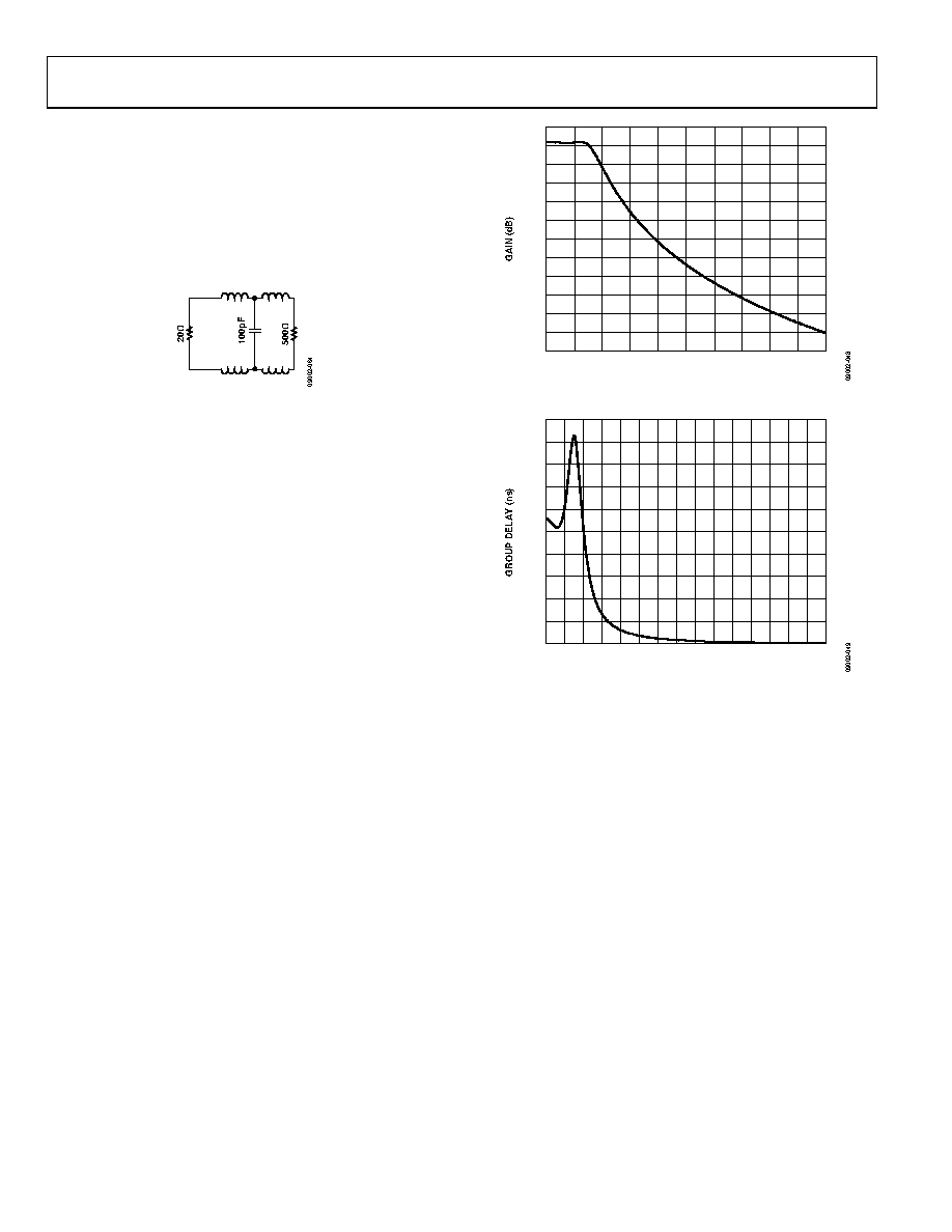 ADRF6510 Rev. 0 | Page 22 of 28 A complete design example is shown in Figure 54. A third-order Chebyshev differential filter with a 31 MHz corner frequency interfaces the output of the ADRF6510 to that of an ADC input. The 20 Ω source impedance reflects the impedance of the output buffer stage. The 500 Ω load resistor defines the input impedance of the ADC. The filter adheres to a 0.1 dB in-band flatness and offers sufficient out-of-band rejection to act as an antialiasing filter. 1.8µH 1.8µH 1µH 1µH Figure 54. Third-Order Chebyshev Differential Filter Design Example Figure 55 and Figure 56 show the measured frequency response and group delay of the third-order Chebyshev differential filter. 10 –50 0 20 40 60 80 100 120 140 200 180 160 BASEBAND FREQUENCY (MHz) –45 –40 –35 –30 –25 –20 –15 –10 –5 0 5 Figure 55. Third-Order Baseband Filter Response 20 0 0 20 40 60 300 280 260 240 220 200 180 160 140 120 100 80 BASEBAND FREQUENCY (MHz) 2 4 6 8 10 12 14 16 18 Figure 56. Third-Order Baseband Filter Group Delay Response |
|
Link URL |
| Does ALLDATASHEET help your business so far? [ DONATE ] |
About Alldatasheet | Advertisement | Contact us | Privacy Policy | Link to Datasheet | Link Exchange | Manufacturer List All Rights Reserved©Alldatasheet.com |
| Russian : Alldatasheetru.com | Korean : Alldatasheet.co.kr | Spanish : Alldatasheet.es | French : Alldatasheet.fr | Italian : Alldatasheetit.com Portuguese : Alldatasheetpt.com | Polish : Alldatasheet.pl | Vietnamese : Alldatasheet.vn Indian : Alldatasheet.in | Mexican : Alldatasheet.com.mx | British : Alldatasheet.co.uk | New Zealand : Alldatasheet.co.nz |
|
Family Site : ic2ic.com |
icmetro.com |
 Indian ▼
 English
 Chinese
 German
 Japanese
 Russian
 Korean
 Spanish
 French
 Italian
 Portuguese
 Polish
 Vietnamese
 Indian
 Mexican
 British
 New Zealand


