|
Electronic Components Datasheet Search |
|
|
Electronic Components Datasheet Search |
|
AD823AARMZ-R7 Datasheet(PDF) 19 Page - Analog Devices |
|
|
|||||||||||||||||||||||||||||
AD823AARMZ-R7 Datasheet(HTML) 19 Page - Analog Devices |
|
|
19 / 20 page 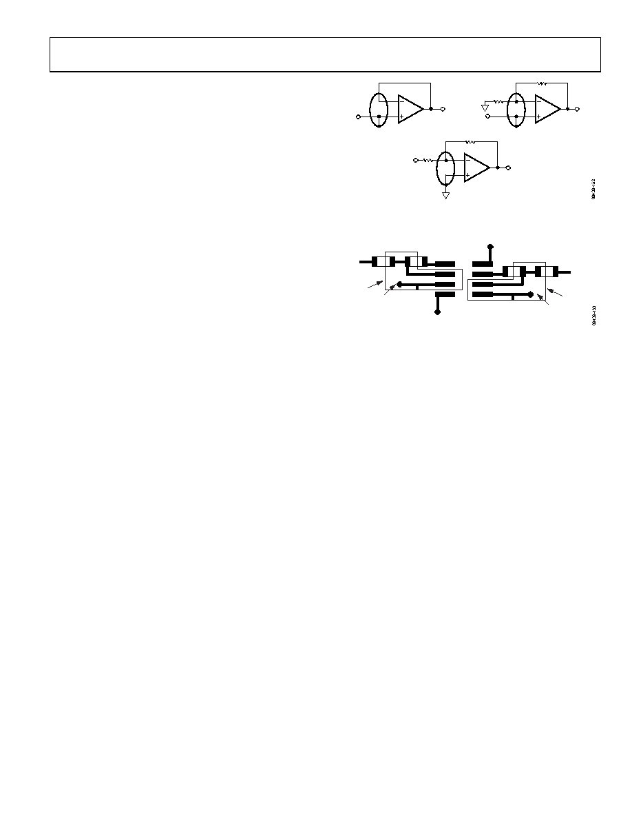 Data Sheet AD823A Rev. | Page 19 of 20 MAXIMIZING PERFORMANCE THROUGH PROPER LAYOUT To achieve the maximum performance of the extremely high input impedance and low offset voltage of the AD823A, care should be taken in the circuit board layout. The PCB surface must remain clean and free of moisture to avoid leakage currents between adjacent traces. Surface coating of the circuit board reduces surface moisture and provides a humidity barrier, reducing parasitic resistance on the board. The use of guard rings around the amplifier inputs further reduces leakage currents. Figure 48 shows how the guard rings should be configured, and Figure 49 shows the top view of how a surface-mount layout can be arranged. The guard ring does not need to be a specific width, but it should form a continuous loop around both inputs. By setting the guard ring voltage equal to the voltage at the non-inverting input, parasitic capacitance is minimized as well. For further reduction of leakage currents, components can be mounted to the PCB using Teflon® standoff insulators. VOUT VOUT VOUT VIN AD823A VIN AD823A VIN AD823A Figure 48. Guard Ring Layout and Connections to Reduce PCB Leakage Currents V– V+ VREF VREF VIN1 VIN2 GUARD RING R1 R2 R2 R1 AD823A GUARD RING Figure 49. Top View of AD823A SOIC Layout with Guard Rings B |
|
|
Link URL |
| Does ALLDATASHEET help your business so far? [ DONATE ] |
About Alldatasheet | Advertisement | Contact us | Privacy Policy | Link to Datasheet | Link Exchange | Manufacturer List All Rights Reserved©Alldatasheet.com |
| Russian : Alldatasheetru.com | Korean : Alldatasheet.co.kr | Spanish : Alldatasheet.es | French : Alldatasheet.fr | Italian : Alldatasheetit.com Portuguese : Alldatasheetpt.com | Polish : Alldatasheet.pl | Vietnamese : Alldatasheet.vn Indian : Alldatasheet.in | Mexican : Alldatasheet.com.mx | British : Alldatasheet.co.uk | New Zealand : Alldatasheet.co.nz |
|
Family Site : ic2ic.com |
icmetro.com |
 Indian ▼
 English
 Chinese
 German
 Japanese
 Russian
 Korean
 Spanish
 French
 Italian
 Portuguese
 Polish
 Vietnamese
 Indian
 Mexican
 British
 New Zealand