|
Electronic Components Datasheet Search |
|
|
Electronic Components Datasheet Search |
|
ST7FOXU0 Datasheet(PDF) 94 Page - STMicroelectronics |
|
|
|||||||||||||||||||||||||||||
ST7FOXU0 Datasheet(HTML) 94 Page - STMicroelectronics |
|
|
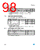
94 / 123 page  Electrical characteristics ST7FOXU0 94/123 Table 40. Current characteristics Symbol Ratings Maximum value Unit IVDD Total current into VDD power lines (source) (1) 1. All power (VDD) and ground (VSS) lines must always be connected to the external supply. 75 mA IVSS Total current out of VSS ground lines (sink) (1) 150 IIO Output current sunk by any standard I/O and control pin 20 Output current sunk by any high sink I/O pin 40 Output current source by any I/Os and control pin - 25 IINJ(PIN) (2)(3) 2. IINJ(PIN) must never be exceeded. This is implicitly insured if VIN maximum is respected. If VIN maximum cannot be respected, the injection current must be limited externally to the IINJ(PIN) value. A positive injection is induced by VIN>VDD while a negative injection is induced by VIN<VSS. For true open-drain pads, there is no positive injection current, and the corresponding VIN maximum must always be respected 3. Negative injection disturbs the analog performance of the device. In particular, it induces leakage currents throughout the device including the analog inputs. To avoid undesirable effects on the analog functions, care must be taken: - Analog input pins must have a negative injection less than 0.8 mA (assuming that the impedance of the analog voltage is lower than the specified limits) - Pure digital pins must have a negative injection less than 1.6 mA. In addition, it is recommended to inject the current as far as possible from the analog input pins. Injected current on RESET pin ± 5 Injected current on OSC1/CLKIN and OSC2 pins ± 5 Injected current on any other pin(4) 4. When several inputs are submitted to a current injection, the maximum ΣI INJ(PIN) is the absolute sum of the positive and negative injected currents (instantaneous values). These results are based on characterization with ΣI INJ(PIN) maximum current injection on four I/O port pins of the device. ± 5 ΣI INJ(PIN) (2) Total injected current (sum of all I/O and control pins)(4) ± 20 Table 41. Thermal characteristics Symbol Ratings Value Unit TSTG Storage temperature range -65 to +150 °C TJ Maximum junction temperature (see Table 66: Thermal characteristics on page 121) |
|
Link URL |
| Does ALLDATASHEET help your business so far? [ DONATE ] |
About Alldatasheet | Advertisement | Contact us | Privacy Policy | Link to Datasheet | Link Exchange | Manufacturer List All Rights Reserved©Alldatasheet.com |
| Russian : Alldatasheetru.com | Korean : Alldatasheet.co.kr | Spanish : Alldatasheet.es | French : Alldatasheet.fr | Italian : Alldatasheetit.com Portuguese : Alldatasheetpt.com | Polish : Alldatasheet.pl | Vietnamese : Alldatasheet.vn Indian : Alldatasheet.in | Mexican : Alldatasheet.com.mx | British : Alldatasheet.co.uk | New Zealand : Alldatasheet.co.nz |
|
Family Site : ic2ic.com |
icmetro.com |
 Indian ▼
 English
 Chinese
 German
 Japanese
 Russian
 Korean
 Spanish
 French
 Italian
 Portuguese
 Polish
 Vietnamese
 Indian
 Mexican
 British
 New Zealand