 |
Electronic Components Datasheet Search |
|
|
Electronic Components Datasheet Search |
|
ADRF6755ACPZ-R7 Datasheet(PDF) 22 Page - Analog Devices |
|
|
|||||||||||||||||||||||||||||
ADRF6755ACPZ-R7 Datasheet(HTML) 22 Page - Analog Devices |
|
|
22 / 48 page 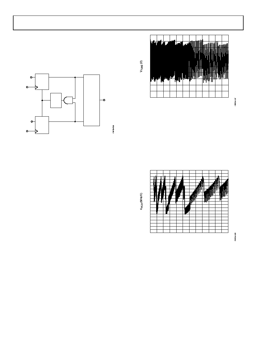 ADRF6755 Data Sheet Rev. B | Page 22 of 48 Phase Frequency Detector (PFD) and Charge Pump The PFD takes inputs from the R-divider and the N-counter and produces an output proportional to the phase and frequency differ- ence between them (see Figure 55 for a simplified schematic). The PFD includes a fixed delay element that sets the width of the antibacklash pulse, ensuring that there is no dead zone in the PFD transfer function. Figure 55. PFD Simplified Schematic Lock Detect (LDET) LDET (Pin 44) signals when the PLL has achieved lock to an error frequency of less than 100 Hz. On a write to Register CR0, a new PLL acquisition cycle starts, and the LDET signal goes low. When lock has been achieved, this signal returns high. Voltage-Controlled Oscillator (VCO) The VCO core in the ADRF6755 consists of three separate VCOs, each with 16 overlapping bands. This configuration of 48 bands allows the VCO frequency range to extend from 2310 MHz to 4800 MHz. The three VCOs are divided by a programmable divider, RFDIV, controlled by Register CR28, Bits[2:0]. This divider provides divisions of 1, 2, 4, 8, and 16 to ensure that the frequency range is extended from 144.375 MHz (2310 MHz/16) to 4800 MHz (4800 MHz/1). A divide-by-2 quadrature circuit in the path to the modulator then provides the full LO frequency range from 100 MHz to 2400 MHz. Figure 56 shows a sweep of VTUNE vs. LO frequency demonstrating the three VCOs overlapping and the multiple overlapping bands within each VCO at the LO frequency range of 100 MHz to 2400 MHz. Note that Figure 56 includes the RFDIV being incorporated to provide further divisions of the fundamental VCO frequency; thus, each VCO is used on multiple different occasions throughout the full LO frequency range. The choice of three 16-band VCOs and an RFDIV allows the wide frequency range to be covered without large VCO sensitivity (KVCO) or resultant poor phase noise and spurious performance. Figure 56. VTUNE vs. LO Frequency The VCO displays a variation of KVCO as VTUNE varies within the band and from band to band. Figure 57 shows how KVCO varies across the full frequency range. Figure 57 is useful when calculating the loop filter bandwidth and individual loop filter components using ADISimPLL™. ADISimPLL is an Analog Devices, Inc., simulator that aids in PLL design, particularly with respect to the loop filter. It reports parameters such as phase noise, integrated phase noise, and acquisition time for a particular set of input conditions. ADISimPLL can be downloaded from www.analog.com/adisimpll. Figure 57. KVCO vs. LO Frequency Autocalibration The correct VCO and band are chosen automatically by the VCO and band select circuitry when Register CR0 is updated. This is referred to as autocalibration. The autocalibration time is set by Register CR25. Autocalibration Time = (BSCDIV × 28)/PFD (3) where: BSCDIV = Register CR25, Bits[7:0]. PFD = PFD frequency. For a PFD frequency of 40 MHz, set BSCDIV = 100 to set an autocalibration time of 70 µs. U3 CLR2 Q2 D2 U2 DOWN UP HI HI CP –IN +IN CHARGE PUMP DELAY CLR1 Q1 D1 U1 0.5 0.7 0.9 1.1 1.3 1.5 1.7 1.9 2.1 2.3 2.5 100 300 500 700 900 1100 1300 1500 1700 1900 2100 2300 2500 LO FREQUENCY (MHz) 0 10 20 30 40 100 300 500 700 900 1100 1300 1500 1700 1900 2100 2300 2500 LO FREQUENCY (MHz) |
|
Link URL |
| Does ALLDATASHEET help your business so far? [ DONATE ] |
About Alldatasheet | Advertisement | Contact us | Privacy Policy | Link to Datasheet | Link Exchange | Manufacturer List All Rights Reserved©Alldatasheet.com |
| Russian : Alldatasheetru.com | Korean : Alldatasheet.co.kr | Spanish : Alldatasheet.es | French : Alldatasheet.fr | Italian : Alldatasheetit.com Portuguese : Alldatasheetpt.com | Polish : Alldatasheet.pl | Vietnamese : Alldatasheet.vn Indian : Alldatasheet.in | Mexican : Alldatasheet.com.mx | British : Alldatasheet.co.uk | New Zealand : Alldatasheet.co.nz |
|
Family Site : ic2ic.com |
icmetro.com |
 Indian ▼
 English
 Chinese
 German
 Japanese
 Russian
 Korean
 Spanish
 French
 Italian
 Portuguese
 Polish
 Vietnamese
 Indian
 Mexican
 British
 New Zealand


