 |
Electronic Components Datasheet Search |
|
|
Electronic Components Datasheet Search |
|
ADL5606ACPZ-R7 Datasheet(PDF) 1 Page - Analog Devices |
|
|
|||||||||||||||||||||||||||||
ADL5606ACPZ-R7 Datasheet(HTML) 1 Page - Analog Devices |
|
|
1 / 18 page 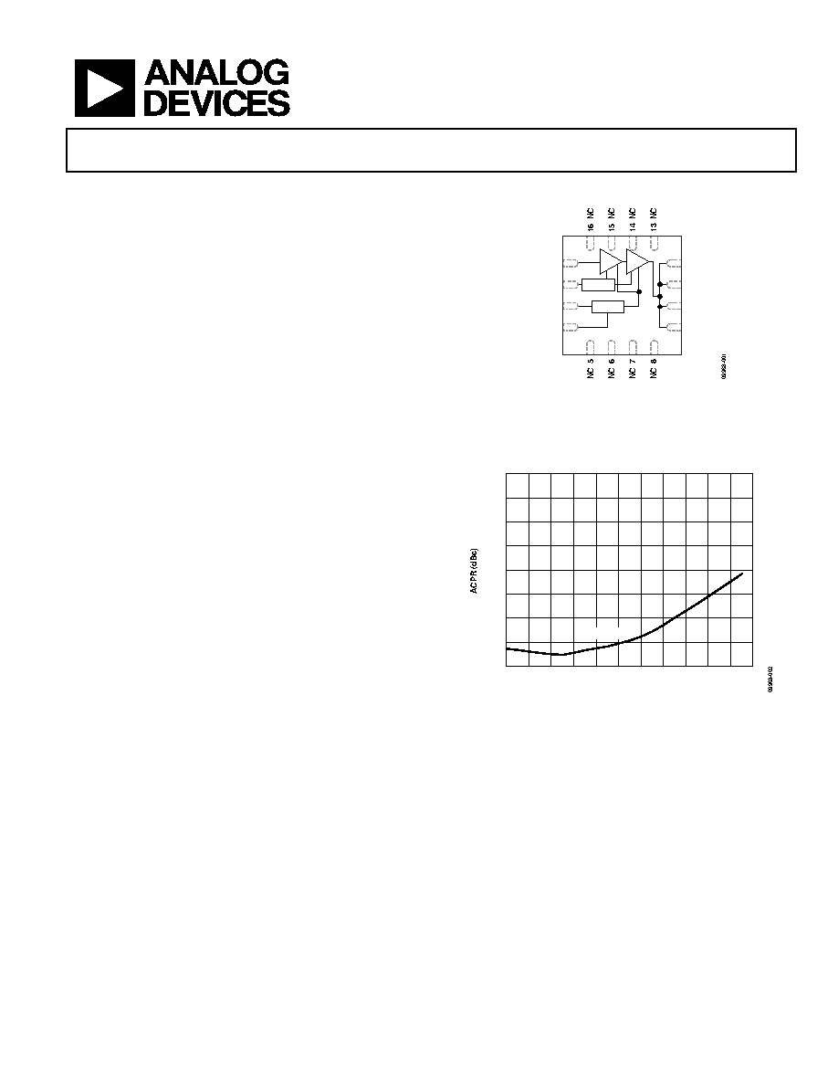 1800 MHz to 2700 MHz, 1 W RF Driver Amplifier Data Sheet ADL5606 Rev. B Document Feedback Information furnished by Analog Devices is believed to be accurate and reliable. However, no responsibilityisassumedbyAnalogDevices for itsuse,nor foranyinfringementsofpatentsor other rightsofthirdpartiesthatmayresultfromitsuse.Specificationssubjecttochangewithoutnotice.No license is granted by implication or otherwise under any patent or patent rights of Analog Devices. Trademarksandregisteredtrademarksarethepropertyoftheirrespectiveowners. One Technology Way, P.O. Box 9106, Norwood, MA 02062-9106, U.S.A. Tel: 781.329.4700 ©2011–2017 Analog Devices, Inc. All rights reserved. Technical Support www.analog.com FEATURES Operation from 1800 MHz to 2700 MHz Gain of 24.3 dB at 2140 MHz OIP3 of 45.5 dBm at 2140 MHz P1dB of 30.8 dBm at 2140 MHz Noise figure of 4.7 dB at 2140 MHz Power supply: 5 V Power supply current: 362 mA typical Internal active biasing Fast power-up/power-down function Compact 4 mm × 4 mm, 16-lead LFCSP ESD rating of ±1 kV (Class 1C) Pin-compatible with the ADL5605 (700 MHz to 1000 MHz) APPLICATIONS Wireless infrastructure Automated test equipment ISM/AMR applications GENERAL DESCRIPTION The ADL5606 is a broadband, two-stage, 1 W RF driver amplifier that operates over a frequency range of 1800 MHz to 2700 MHz. The device can be used in a wide variety of wired and wireless applications, including ISM, MC-GSM, W-CDMA, TD-SCDMA, and LTE. The ADL5606 operates on a 5 V supply voltage and a supply current of 362 mA. The driver also incorporates a fast power- up/power-down function for TDD applications, applications that require a power saving mode, and applications that intermittently transmit data. The ADL5606 is fabricated on a GaAs HBT process and is packaged in a compact 4 mm × 4 mm, 16-lead LFCSP that uses an exposed paddle for excellent thermal impedance. The ADL5606 operates from −40°C to +85°C. A fully populated evaluation board tuned to 2140 MHz is also available. FUNCTIONAL BLOCK DIAGRAM 11 RFOUT 12 RFOUT 10 RFOUT 9 RFOUT 1 RFIN 2 DISABLE 3 VCC 4 VBIAS ADL5606 VBIAS PWDN Figure 1. 0 –80 –70 –60 –50 –40 –30 –20 –10 0 2 4 6 8 10 12 14 16 18 20 22 POUT (dBm) 2140 MHz Figure 2. ACPR vs. Output Power, 3GPP, TM1-64, at 2140 MHz |
Similar Part No. - ADL5606ACPZ-R7 |
|
Similar Description - ADL5606ACPZ-R7 |
|
|
|
Link URL |
| Does ALLDATASHEET help your business so far? [ DONATE ] |
About Alldatasheet | Advertisement | Contact us | Privacy Policy | Link to Datasheet | Link Exchange | Manufacturer List All Rights Reserved©Alldatasheet.com |
| Russian : Alldatasheetru.com | Korean : Alldatasheet.co.kr | Spanish : Alldatasheet.es | French : Alldatasheet.fr | Italian : Alldatasheetit.com Portuguese : Alldatasheetpt.com | Polish : Alldatasheet.pl | Vietnamese : Alldatasheet.vn Indian : Alldatasheet.in | Mexican : Alldatasheet.com.mx | British : Alldatasheet.co.uk | New Zealand : Alldatasheet.co.nz |
|
Family Site : ic2ic.com |
icmetro.com |
 Indian ▼
 English
 Chinese
 German
 Japanese
 Russian
 Korean
 Spanish
 French
 Italian
 Portuguese
 Polish
 Vietnamese
 Indian
 Mexican
 British
 New Zealand


