|
Electronic Components Datasheet Search |
|
|
Electronic Components Datasheet Search |
|
AD8342ACPZ-R2 Datasheet(PDF) 15 Page - Analog Devices |
|
|
|||||||||||||||||||||||||||||
AD8342ACPZ-R2 Datasheet(HTML) 15 Page - Analog Devices |
|
|
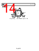
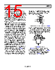
15 / 25 page 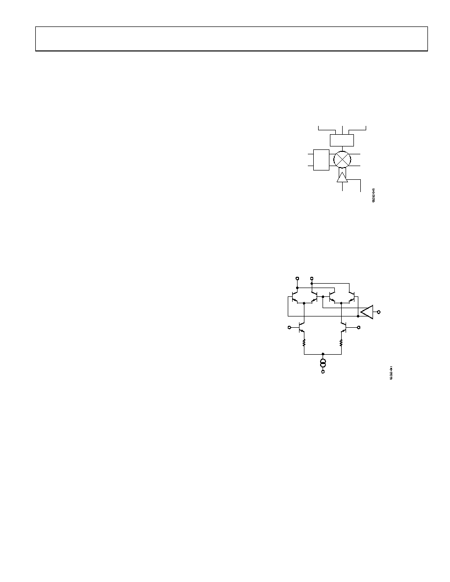 Data Sheet AD8342 Rev. C | Page 15 of 25 THEORY OF OPERATION The AD8342 is an active mixer, optimized for operation within the RF input frequency range of near dc to 3.8 GHz. It has a differential, high impedance RF input that can be terminated or matched externally. The RF input can be driven either single-ended or differentially. The LO input is a single-ended 50 Ω input. The IF outputs are differential open-collectors. The mixer current can be adjusted by the value of an external resistor to optimize performance for gain, compression, and intermodulation, or for low power operation. Figure 39 shows the basic blocks of the mixer, including the LO buffer, RF voltage-to-current converter, bias cell, and mixing core. The RF voltage to RF current conversion is done via a resistively degenerated differential pair. To drive this port single-ended, the RFCM pin must be ac grounded and the RFIN pin ac-coupled to the signal source. The RF inputs can also be driven differentially. The voltage to current converter then drives the emitters of a four-transistor switching core. This switching core is driven by an amplified version of the local oscillator signal connected to the LO input. There are three limiting gain stages between the external LO signal and the switching core. The first stage converts the single-ended LO drive to a well-balanced differential drive. The differential drive then passes through two more gain stages, which ensures that a limited signal drives the switching core. This affords the user a lower LO drive requirement, while maintaining excellent distortion and compression performance. The output signal of these three LO gain stages drives the four transistors within the mixer core to commutate at the rate of the local oscillator frequency. The output of the mixer core is taken directly from its open-collectors. The open-collector outputs present a high impedance at the IF frequency. The conversion gain of the mixer depends directly on the impedance presented to these open-collectors. In characterization, a 100 Ω load was presented to the device via a 2:1 impedance transformer. The device also features a power-down function. Application of a logic low at the PWDN pin allows normal operation. A high logic level at the PWDN pin shuts down the AD8342. Power consumption when the device is disabled is less than 10 mW. The bias for the mixer is set with an external resistor (RBIAS) from the EXRB pin to ground. The value of this resistor directly affects the dynamic range of the mixer. The external resistor must not be lower than 1.82 kΩ. Permanent damage to the device can result if values below 1.8 kΩ are used. This resistor sets the dc current through the mixer core. The performance effects of changing this resistor can be seen in the Typical Performance Characteristics section. LO INPUT VPLO IFOP IFOM RFIN RFCM BIAS EXTERNAL BIAS RESISTOR VPDC PWDN V TO I Figure 39. Simplified Schematic Showing the Key Elements of the AD8342 As shown in Figure 40, the IF output pins, IFOP and IFOM, are directly connected to the open-collectors of the NPN transistors in the mixer core so the differential and single-ended impedances looking into this port are relatively high, on the order of several kΩ. A connection between the supply voltage and these output pins is required for proper mixer core operation. IFOP IFOM LOIN RFCM RFIN COMM Figure 40. AD8342 Simplified Schematic The AD8342 has three pins for the supply voltage: VPDC, VPMX, and VPLO. These pins are separated to minimize or eliminate possible parasitic coupling paths within the AD8342 that can cause spurious signals or reduced interport isolation. Consequently, each of these pins must be well bypassed and decoupled as close to the AD8342 as possible. |
|
|
Link URL |
| Does ALLDATASHEET help your business so far? [ DONATE ] |
About Alldatasheet | Advertisement | Contact us | Privacy Policy | Link to Datasheet | Link Exchange | Manufacturer List All Rights Reserved©Alldatasheet.com |
| Russian : Alldatasheetru.com | Korean : Alldatasheet.co.kr | Spanish : Alldatasheet.es | French : Alldatasheet.fr | Italian : Alldatasheetit.com Portuguese : Alldatasheetpt.com | Polish : Alldatasheet.pl | Vietnamese : Alldatasheet.vn Indian : Alldatasheet.in | Mexican : Alldatasheet.com.mx | British : Alldatasheet.co.uk | New Zealand : Alldatasheet.co.nz |
|
Family Site : ic2ic.com |
icmetro.com |
 Indian ▼
 English
 Chinese
 German
 Japanese
 Russian
 Korean
 Spanish
 French
 Italian
 Portuguese
 Polish
 Vietnamese
 Indian
 Mexican
 British
 New Zealand