|
Electronic Components Datasheet Search |
|
|
Electronic Components Datasheet Search |
|
AD8342ACPZ-R2 Datasheet(PDF) 20 Page - Analog Devices |
|
|
|||||||||||||||||||||||||||||
AD8342ACPZ-R2 Datasheet(HTML) 20 Page - Analog Devices |
|
|
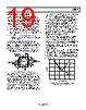
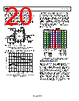
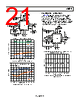
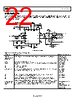
20 / 25 page 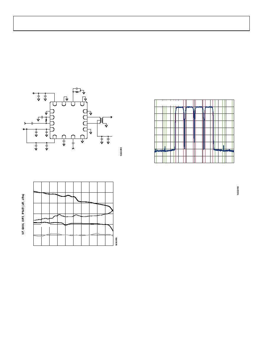 AD8342 Data Sheet Rev. C | Page 20 of 25 The available frequency range of the AD8342 is extremely broad. With adequate care, any of the mixer ports can be optimized for extremely low frequencies, or up to several GHz. The standard evaluation board is populated for broadband performance from a few MHz to ~1 GHz. The input match of the RF port degrades at higher frequencies when using the standard eval board. The broadband frequency range can be extended by minimizing parasitics between the input terminating resistor, R5, and the input pins. 8 7 6 13 15 16 COMM IFOP IFOM 5 COMM 14 2 1 3 4 COMM RFCM RFIN VPMX VPDC PWDN EXRB COMM 11 12 10 9 VPLO LOCM LOIN COMM AD8342 VPOS 1000pF 1000pF 0.1µF VPOS 1nF 1nF LO IN 1.82kΩ 100pF RF IN 1nF 100Ω VPOS 1000pF 0.1µF 1nF 0.1µF 100pF IF OUT (190MHz) TC2-1T 0.1µF NOTES 1. INPUT TERMINATION PLACED AS CLOSE AS POSSIBLE TO RFIN AND RFCM INPUTS. Figure 53. Modified Evaluation Board Schematic for Broadband Downconversion Performance up to 3 GHz The measurements in Figure 54 were made using the modified evaluation board as configured in Figure 53. 30 0 500 3000 RF FREQUENCY (MHz) 25 20 15 10 5 1000 1500 2000 2500 NF GAIN OIP3 IP1dB Figure 54. Input OIP3, Input P1dB, Gain, and NF vs. RF Frequency for a 190 MHz IF Using a Low-Side LO The broadband frequency capabilities of the AD8342 makes it an attractive solution for a variety of applications, including cellular, CATV, point-to-point radio links, and test equipment. As an example, the circuit depicted in Figure 53 can easily be applied as a feedback mixer in a predistortion receiver design. The performance depicted in Figure 55 was measured using a 160 MHz IF. Here, four W-CDMA carriers with high PAR are downconverted for IF sampling so that transmit path nonlinearities can be measured and minimized using digital predistortion techniques. –30 CENTER 160MHz SPAN 40.6MHz –50 –40 –70 –60 –90 –80 –110 –100 –120 4.06MHz POS –22.564dBm REF –22.6dBm ATT 5dB RBW 30kHz VBW 300kHz SWT 4s STANDARD: W-CDMA 3GPP FWD Tx CHANNELS CH1 (REF) –20.65dBm CH2 –20.29dBm CH3 –20.25dBm CH4 –20.29dBm TOTAL –14.35dBm ADJACENT CHANNE L LOWER –61.36dB UPPER –60.84dB ALTERNATE CHANNEL LOWER –61.94dB UPPER –61.72dB Figure 55. ACPR Performance for Multiple W-CDMA Carriers Being Downconverted from 2140 MHz to 160 MHz for Distortion Analysis APPLICATIONS ABOVE 3 GHZ Operation of the AD8342 mixer can be extended above 3 GHz; however, bandwidth is limited due to on-chip parasitics. By eliminating all unnecessary parasitics in the LO path, the LO input voltage standing wave ratio (VSWR) can be kept low up to 4 GHz. Figure 56 shows the circuit configuration for the RF input frequency of 3.5 GHz to 3.8 GHz. A 22 Ω resistor is added between the RFCM pin and the 1 nF capacitor to ground, and a 1 pF capacitor is also added to provide the tuning for the desired frequency range. The resulting RF and LO input return losses are shown in Figure 57. Using a fixed LO frequency of 3.4 GHz, the conversion gain response for the RF input frequency range from 3.5 GHz to 3.8 GHz is shown in Figure 59. |
|
|
Link URL |
| Does ALLDATASHEET help your business so far? [ DONATE ] |
About Alldatasheet | Advertisement | Contact us | Privacy Policy | Link to Datasheet | Link Exchange | Manufacturer List All Rights Reserved©Alldatasheet.com |
| Russian : Alldatasheetru.com | Korean : Alldatasheet.co.kr | Spanish : Alldatasheet.es | French : Alldatasheet.fr | Italian : Alldatasheetit.com Portuguese : Alldatasheetpt.com | Polish : Alldatasheet.pl | Vietnamese : Alldatasheet.vn Indian : Alldatasheet.in | Mexican : Alldatasheet.com.mx | British : Alldatasheet.co.uk | New Zealand : Alldatasheet.co.nz |
|
Family Site : ic2ic.com |
icmetro.com |
 Indian ▼
 English
 Chinese
 German
 Japanese
 Russian
 Korean
 Spanish
 French
 Italian
 Portuguese
 Polish
 Vietnamese
 Indian
 Mexican
 British
 New Zealand