 |
Electronic Components Datasheet Search |
|
|
Electronic Components Datasheet Search |
|
STM32W108HB Datasheet(PDF) 89 Page - STMicroelectronics |
|
|
|||||||||||||||||||||||||||||
STM32W108HB Datasheet(HTML) 89 Page - STMicroelectronics |
|
|
89 / 278 page 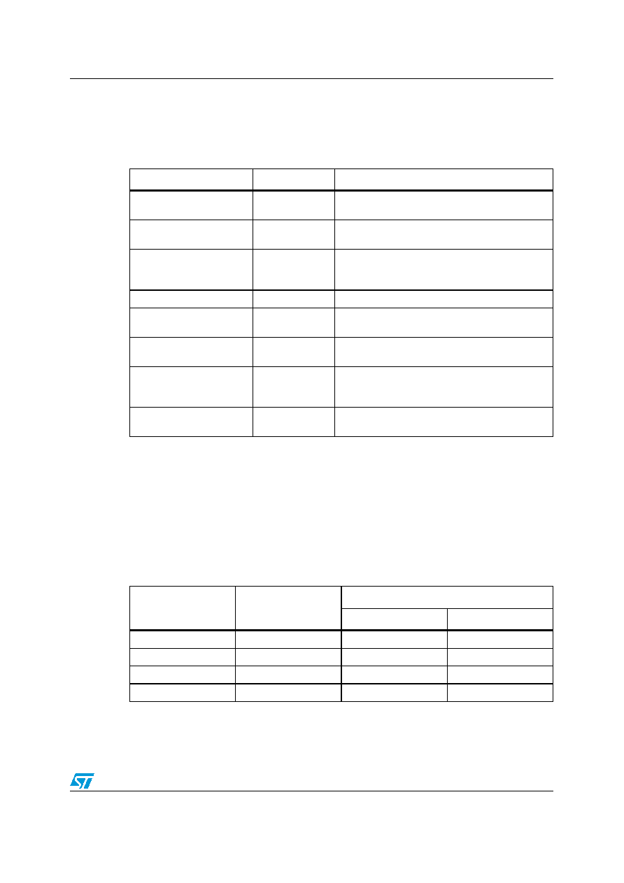 STM32W108HB STM32W108CC STM32W108CB STM32W108CZ General-purpose input/output Doc ID 16252 Rev 14 89/278 8.1.2 Configuration Each pin has a 4-bit configuration value in the GPIOx_CRH/L register. The various GPIO modes and their 4 bit configuration values are shown in Table 13. Analog Analog input or output. When in analog mode, the digital input (GPIOx_IDR) always reads 1. Input (floating) Digital input without an internal pull up or pull down. Output is disabled. Input (pull-up or pull-down) Digital input with an internal pull up or pull down. A set bit in GPIOx_ODR selects pull up and a cleared bit selects pull down. Output is disabled. Output (push-pull) Push-pull output. GPIOx_ODR controls the output. Output (open-drain) Open-drain output. GPIOx_ODR controls the output. If a pull up is required, it must be external. Alternate Output (push-pull) Push-pull output. An onboard peripheral controls the output. Alternate Output (open-drain) 0xD Open-drain output. An onboard peripheral controls the output. If a pull up is required, it must be external. Alternate Output (push-pull) SPI SCLK Mode 0xB Push-pull output mode only for SPI master mode SCLK pins. If a GPIO has two peripherals that can be the source of alternate output mode data, then other registers in addition to GPIOx_CRH/L determine which peripheral controls the output. Several GPIOs share an alternate output with Timer 2 and the Serial Controllers. Bits in Timer 2's TIM2_OR register control routing Timer 2 outputs to different GPIOs. Bits in Timer 2's TIM2_CCER register enable Timer 2 outputs. When Timer 2 outputs are enabled they override Serial Controller outputs. Table 14 indicates the GPIO mapping for Timer 2 outputs depending on the bits in the register TIM2_OR. Refer to Section 10: General-purpose timers on page 155 for complete information on timer configuration. For outputs assigned to the serial controllers, the serial interface mode registers (SCx_CR) determine how the GPIO pins are used. Table 13. GPIO configuration modes GPIO mode GPIOx_CRH/L Description 0x0 0x4 0x8 0x1 0x5 0x9 Table 14. Timer 2 output configuration controls Timer 2 output Option register bit GPIO mapping selected by TIM2_OR bit 01 TIM2_CH1 TIM2_OR[4] PA0 PB1 TIM2_CH2 TIM2_OR[5] PA3 PB2 TIM2_CH3 TIM2_OR[6] PA1 PB3 TIM2_CH4 TIM2_OR[7] PA2 PB4 |
|
Link URL |
| Does ALLDATASHEET help your business so far? [ DONATE ] |
About Alldatasheet | Advertisement | Contact us | Privacy Policy | Link to Datasheet | Link Exchange | Manufacturer List All Rights Reserved©Alldatasheet.com |
| Russian : Alldatasheetru.com | Korean : Alldatasheet.co.kr | Spanish : Alldatasheet.es | French : Alldatasheet.fr | Italian : Alldatasheetit.com Portuguese : Alldatasheetpt.com | Polish : Alldatasheet.pl | Vietnamese : Alldatasheet.vn Indian : Alldatasheet.in | Mexican : Alldatasheet.com.mx | British : Alldatasheet.co.uk | New Zealand : Alldatasheet.co.nz |
|
Family Site : ic2ic.com |
icmetro.com |
 Indian ▼
 English
 Chinese
 German
 Japanese
 Russian
 Korean
 Spanish
 French
 Italian
 Portuguese
 Polish
 Vietnamese
 Indian
 Mexican
 British
 New Zealand


