|
Electronic Components Datasheet Search |
|
|
Electronic Components Datasheet Search |
|
LQFP64 Datasheet(PDF) 62 Page - STMicroelectronics |
|
|
|||||||||||||||||||||||||||||
LQFP64 Datasheet(HTML) 62 Page - STMicroelectronics |
|
|
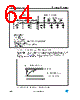
62 / 90 page  Electrical characteristics SPC560D30x, SPC56040Dx 62/90 Doc ID 16315 Rev 7 4.17.2 Input impedance and ADC accuracy In the following analysis, the input circuit corresponding to the precise channels is considered. To preserve the accuracy of the A/D converter, it is necessary that analog input pins have low AC impedance. Placing a capacitor with good high frequency characteristics at the input pin of the device can be effective: the capacitor should be as large as possible, ideally infinite. This capacitor contributes to attenuating the noise present on the input pin; furthermore, it sources charge during the sampling phase, when the analog signal source is a high-impedance source. A real filter can typically be obtained by using a series resistance with a capacitor on the input pin (simple RC filter). The RC filtering may be limited according to the value of source impedance of the transducer or circuit supplying the analog signal to be measured. The filter at the input pins must be designed taking into account the dynamic characteristics of the input signal (bandwidth) and the equivalent input impedance of the ADC itself. In fact a current sink contributor is represented by the charge sharing effects with the sampling capacitance: being CS and Cp2 substantially two switched capacitances, with a frequency equal to the conversion rate of the ADC, it can be seen as a resistive path to ground. For instance, assuming a conversion rate of 1 MHz, with CS+Cp2 equal to 3 pF, a resistance of 330 k is obtained (R EQ = 1 / (fc ×(CS+Cp2)), where fc represents the conversion rate at the considered channel). To minimize the error induced by the voltage partitioning between this resistance (sampled voltage on CS+Cp2) and the sum of RS + RF, the external circuit must be designed to respect the Equation 4: Equation 4 Equation 4 generates a constraint for external network design, in particular on a resistive path. V A R S R F + R EQ --------------------- 1 2 ---LSB |
|
Link URL |
| Does ALLDATASHEET help your business so far? [ DONATE ] |
About Alldatasheet | Advertisement | Contact us | Privacy Policy | Link to Datasheet | Link Exchange | Manufacturer List All Rights Reserved©Alldatasheet.com |
| Russian : Alldatasheetru.com | Korean : Alldatasheet.co.kr | Spanish : Alldatasheet.es | French : Alldatasheet.fr | Italian : Alldatasheetit.com Portuguese : Alldatasheetpt.com | Polish : Alldatasheet.pl | Vietnamese : Alldatasheet.vn Indian : Alldatasheet.in | Mexican : Alldatasheet.com.mx | British : Alldatasheet.co.uk | New Zealand : Alldatasheet.co.nz |
|
Family Site : ic2ic.com |
icmetro.com |
 Indian ▼
 English
 Chinese
 German
 Japanese
 Russian
 Korean
 Spanish
 French
 Italian
 Portuguese
 Polish
 Vietnamese
 Indian
 Mexican
 British
 New Zealand