|
Electronic Components Datasheet Search |
|
|
Electronic Components Datasheet Search |
|
LQFP64 Datasheet(PDF) 71 Page - STMicroelectronics |
|
|
|||||||||||||||||||||||||||||
LQFP64 Datasheet(HTML) 71 Page - STMicroelectronics |
|
|
71 / 90 page 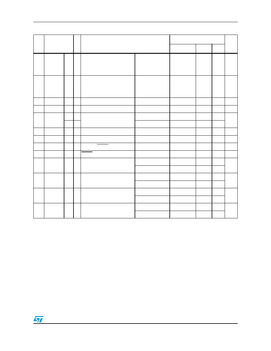 SPC560D30x, SPC56040Dx Electrical characteristics Doc ID 16315 Rev 7 71/90 — t CSC CC D Internal delay between pad associated to SCK and pad associated to CSn in master mode Master mode — — 130(2) ns — t ASC CC D Internal delay between pad associated to SCK and pad associated to CSn in master mode for CSn1 1 Master mode — — 130(2) ns 2tCSCext (3) SR D CS to SCK delay Slave mode 32 — — ns 3tASCext (4) SR D After SCK delay Slave mode 1/fDSPI + 5 — — ns 4tSDC CC D SCK duty cycle Master mode — tSCK/2 — ns SR D Slave mode tSCK/2 — — 5tA SR D Slave access time — 1/fDSPI +70 — — ns 6tDI SR D Slave SOUT disable time — 7 — — ns 7tPCSC SR D PCSx to PCSS time — 0 — — ns 8tPASC SR D PCSS to PCSx time — 0 — — ns 9tSUI SR D Data setup time for inputs Master mode 43 — — ns Slave mode 5 — — 10 tHI SR D Data hold time for inputs Master mode 0 — — ns Slave mode 2(5) —— 11 tSUO (6) CC D Data valid after SCK edge Master mode — — 32 ns Slave mode — — 52 12 tHO (6) CC D Data hold time for outputs Master mode 0 — — ns Slave mode 8 — — 1. Operating conditions: COUT = 10 to 50 pF, SlewIN = 3.5 to 15 ns 2. Maximum is reached when CSn pad is configured as SLOW pad while SCK pad is configured as MEDIUM pad 3. The tCSC delay value is configurable through a register. When configuring tCSC (using PCSSCK and CSSCK fields in DSPI_CTARx registers), delay between internal CS and internal SCK must be higher than t CSC to ensure positive tCSCext. 4. The tASC delay value is configurable through a register. When configuring tASC (using PASC and ASC fields in DSPI_CTARx registers), delay between internal CS and internal SCK must be higher than t ASC to ensure positive tASCext. 5. This delay value corresponds to SMPL_PT = 00b which is bit field 9 and 8 of DSPI_MCR. 6. SCK and SOUT configured as MEDIUM pad Table 44. DSPI characteristics(1) (continued) No. Symbol C Parameter DSPI0/DSPI1 Unit Min Typ Max |
|
Link URL |
| Does ALLDATASHEET help your business so far? [ DONATE ] |
About Alldatasheet | Advertisement | Contact us | Privacy Policy | Link to Datasheet | Link Exchange | Manufacturer List All Rights Reserved©Alldatasheet.com |
| Russian : Alldatasheetru.com | Korean : Alldatasheet.co.kr | Spanish : Alldatasheet.es | French : Alldatasheet.fr | Italian : Alldatasheetit.com Portuguese : Alldatasheetpt.com | Polish : Alldatasheet.pl | Vietnamese : Alldatasheet.vn Indian : Alldatasheet.in | Mexican : Alldatasheet.com.mx | British : Alldatasheet.co.uk | New Zealand : Alldatasheet.co.nz |
|
Family Site : ic2ic.com |
icmetro.com |
 Indian ▼
 English
 Chinese
 German
 Japanese
 Russian
 Korean
 Spanish
 French
 Italian
 Portuguese
 Polish
 Vietnamese
 Indian
 Mexican
 British
 New Zealand