 |
Electronic Components Datasheet Search |
|
|
Electronic Components Datasheet Search |
|
EM357-RTR Datasheet(PDF) 146 Page - List of Unclassifed Manufacturers |
|
|
|||||||||||||||||||||||||||||
EM357-RTR Datasheet(HTML) 146 Page - List of Unclassifed Manufacturers |
|
|
146 / 240 page 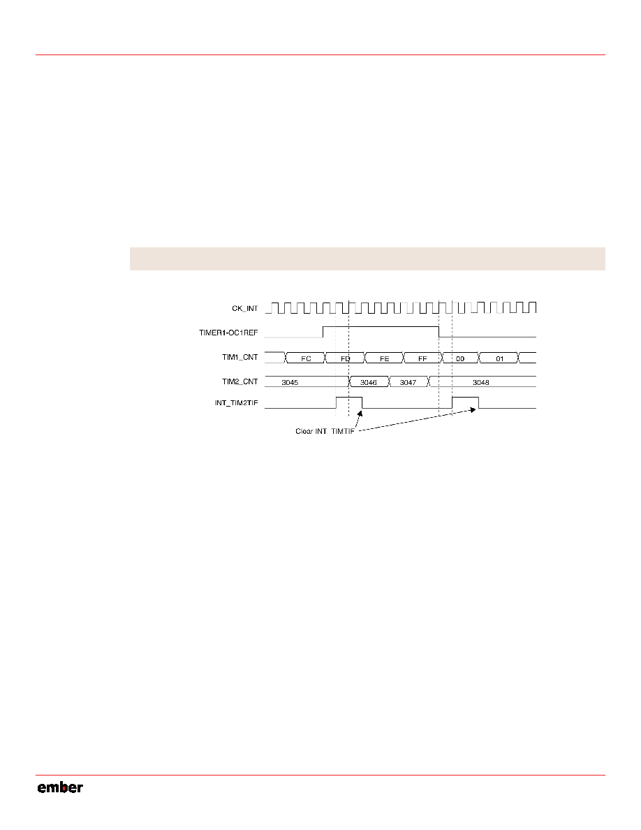 EM351 / EM357 9.3.14.2 Using One Timer to Enable the Other Timer In this example, shown in Figure 9-32, the enable of Timer 2 is controlled with the output compare 1 of Timer 1. Timer 2 counts on the divided internal clock only when OC1REF of Timer 1 is high. Both counter clock frequencies are divided by 3 by the prescaler compared to CK_INT (fCK_CNT = fCK_INT /3). Configure Timer 1 in master mode to send its Output Compare Reference (OC1REF) signal as trigger output: Write TIM_MMS = 100 in the TIM1_CR2 register. Configure the Timer 1 OC1REF waveform (TIM1_CCMR1 register). Configure Timer 2 to get the input trigger from Timer 1: Write TIM_TS = 000 in the TIM2_SMCR register. Configure Timer 2 in gated mode: Write TIM_SMS = 101 in the TIM2_SMCR register. Enable Timer 2: Write 1 in the TIM_CEN bit in the TIM2_CR1 register. Start Timer 1: Write 1 in the TIM_CEN bit in the TIM1_CR1 register. Note: The counter 2 clock is not synchronized with counter 1, this mode only affects the Timer 2 counter enable signal. Figure 9-32. Gating Timer 2 with OC1REF of Timer 1 In the example in Figure 9-32, the Timer 2 counter and prescaler are not initialized before being started. So they start counting from their current value. It is possible to start from a given value by resetting both timers before starting Timer 1, then writing the desired value in the timer counters. The timers can easily be reset by software using the TIM_UG bit in the TIMx_EGR registers. The next example, illustrated in Figure 9-33, synchronizes Timer 1 and Timer 2. Timer 1 is the master and starts from 0. Timer 2 is the slave and starts from 0xE7. The prescaler ratio is the same for both timers. Timer 2 stops when Timer 1 is disabled by writing 0 to the TIM_CEN bit in the TIM1_CR1 register: Configure Timer 1 in master mode to send its Output Compare Reference (OC1REF) signal as trigger output: Write TIM_MMS = 100 in the TIM1_CR2 register) Configure the Timer 1 OC1REF waveform (TIM1_CCMR1 register). Configure Timer 2 to get the input trigger from Timer 1: Write TIM_TS = 000 in the TIM2_SMCR register. Configure Timer 2 in gated mode: Write TIM_SMS = 101 in the TIM2_SMCR register. Reset Timer 1: Write 1 in the TIM_UG bit (TIM1_EGR register. Reset Timer 2 by writing 1 in the TIM_UG bit (TIM2_EGR register). Initialize Timer 2 to 0xE7: Write 0xE7 in the Timer 2 counter (TIM2_CNTL). Enable Timer 2: Write 1 in the TIM_CEN bit in the TIM2_CR1 register. Start Timer 1: Write 1 in the TIM_CEN bit in the TIM1_CR1 register. Stop Timer 1: Write 0 in the TIM_CEN bit in the TIM1_CR1 register. 9-26 120-035X-000D Preliminary |
|
Link URL |
| Does ALLDATASHEET help your business so far? [ DONATE ] |
About Alldatasheet | Advertisement | Contact us | Privacy Policy | Link to Datasheet | Link Exchange | Manufacturer List All Rights Reserved©Alldatasheet.com |
| Russian : Alldatasheetru.com | Korean : Alldatasheet.co.kr | Spanish : Alldatasheet.es | French : Alldatasheet.fr | Italian : Alldatasheetit.com Portuguese : Alldatasheetpt.com | Polish : Alldatasheet.pl | Vietnamese : Alldatasheet.vn Indian : Alldatasheet.in | Mexican : Alldatasheet.com.mx | British : Alldatasheet.co.uk | New Zealand : Alldatasheet.co.nz |
|
Family Site : ic2ic.com |
icmetro.com |
 Indian ▼
 English
 Chinese
 German
 Japanese
 Russian
 Korean
 Spanish
 French
 Italian
 Portuguese
 Polish
 Vietnamese
 Indian
 Mexican
 British
 New Zealand


