 |
Electronic Components Datasheet Search |
|
|
Electronic Components Datasheet Search |
|
The question interval is too short.
Please try again in a few seconds.

Hello, Please ask a question about AS3661 Datasheet
# Example questions:
➢ What is the typical switching frequency (fsw) of the charge pump?
➢ What is the recommended maximum charge pump load current (iload)?
➢ What is the typical standby supply current (ivbat) when the chip is disabled (en = 0v or chip_en=0) and the external 32 khz clock is running or not running?
| Part No. | AS3661 |
| Manufacturer | AMSCO |
| Size | 3Mb |
| Pages | 87 pages |
| Description | Programmable 9-channel LED Dr iver |






















1. General Operating Conditions
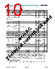
️· Supply Voltage (VBAT): 2.7V to 5.5V
️· Standby Supply Current (IVBAT - EN=0): 1.4 µA to 4 µA (with external 32kHz clock running or not)
️· Normal Mode Supply Current (External 32kHz clock running, outputs disabled): 0.16 mA to 0.22 mA
️· Power Save Mode Supply Current (External 32kHz clock running): 3.1 µA to 5 µA
️· Internal Oscillator Frequency Accuracy:
- -4% to +4% at 25°C
- -7% to +7%
️· Operating Temperature: -30°C to +85°C
2. Charge Pump Parameters
️· Charge Pump Output Resistance (ROUT): Varies depending on gain and VBAT voltage:
- Gain = 1.5, VBAT = 2.9V: 6 Ω
- Gain = 1, VBAT = 2.9V: 1 Ω
- Gain = 1.5, VBAT = 3.6V: 1.4 Ω
- Gain = 1, VBAT = 3.6V: 1 Ω
️· Switching Frequency (fSW): 1.2 MHz to 1.3 MHz
️· Ground Current (IGND): 1.2 mA to 2.5 mA
️· VCP Turn-On Time: 100 µs
️· Recommended Charge Pump Load Current: 0 mA to 100 mA
3. LED Driver Parameters
️· Leakage Current (ILEAK - PWM=0%): 0.1 µA to 1 µA (per LED output)
️· Maximum Source Current (IMAX): 25.5 mA (per LED output)
️· Output Current Accuracy (at 17.5mA, 25°C): -2.5% to +2.5%
️· Output Current Accuracy (at 17.5mA): -5% to +5%
️· Matching Accuracy (LED output current): 1% to 2.5%
️· LED Switching Frequency (fLED): 312 Hz
️· Saturation Voltage (VSAT - at 17.5mA): 45mV to 100mV
IMPORTANT NOTES & CAVEATS:
️· Typical vs. Minimum/Maximum: The datasheet excerpt emphasizes *minimum* and *maximum* values. "Typ" values are typical values and not guaranteed. Design should not rely solely on "Typ" values.
️· Conditions: *Read the conditions associated with each parameter.* The values are only valid *if* the specified conditions are met. Varying conditions (temperature, voltage, load) will alter the parameter values.
️· Gain: The charge pump output resistance (ROUT) is heavily dependent on the gain setting. Be certain to account for this when designing your circuit.
️· Application: This is an excerpt; it doesn't describe the entire functionality. Consult the full datasheet for complete details, application notes, and layout recommendations.
️· Footnotes: Pay very close attention to the footnotes in the original data sheet. They define the conditions and test setups used to obtain the given values.
️· Design margin: It's crucial to include sufficient design margin. The datasheet provides minimum and maximum values. Real-world performance can vary, so avoid operating close to these limits.
1. General Operating Conditions
️· Supply Voltage (VBAT): 2.7V to 5.5V
️· Standby Supply Current (IVBAT - EN=0): 1.4 µA to 4 µA (with external 32kHz clock running or not)
️· Normal Mode Supply Current (External 32kHz clock running, outputs disabled): 0.16 mA to 0.22 mA
️· Power Save Mode Supply Current (External 32kHz clock running): 3.1 µA to 5 µA
️· Internal Oscillator Frequency Accuracy:
- -4% to +4% at 25°C
- -7% to +7%
️· Operating Temperature: -30°C to +85°C
2. Charge Pump Parameters
️· Charge Pump Output Resistance (ROUT): Varies depending on gain and VBAT voltage:
- Gain = 1.5, VBAT = 2.9V: 6 Ω
- Gain = 1, VBAT = 2.9V: 1 Ω
- Gain = 1.5, VBAT = 3.6V: 1.4 Ω
- Gain = 1, VBAT = 3.6V: 1 Ω
️· Switching Frequency (fSW): 1.2 MHz to 1.3 MHz
️· Ground Current (IGND): 1.2 mA to 2.5 mA
️· VCP Turn-On Time: 100 µs
️· Recommended Charge Pump Load Current: 0 mA to 100 mA
3. LED Driver Parameters
️· Leakage Current (ILEAK - PWM=0%): 0.1 µA to 1 µA (per LED output)
️· Maximum Source Current (IMAX): 25.5 mA (per LED output)
️· Output Current Accuracy (at 17.5mA, 25°C): -2.5% to +2.5%
️· Output Current Accuracy (at 17.5mA): -5% to +5%
️· Matching Accuracy (LED output current): 1% to 2.5%
️· LED Switching Frequency (fLED): 312 Hz
️· Saturation Voltage (VSAT - at 17.5mA): 45mV to 100mV
IMPORTANT NOTES & CAVEATS:
️· Typical vs. Minimum/Maximum: The datasheet excerpt emphasizes *minimum* and *maximum* values. "Typ" values are typical values and not guaranteed. Design should not rely solely on "Typ" values.
️· Conditions: *Read the conditions associated with each parameter.* The values are only valid *if* the specified conditions are met. Varying conditions (temperature, voltage, load) will alter the parameter values.
️· Gain: The charge pump output resistance (ROUT) is heavily dependent on the gain setting. Be certain to account for this when designing your circuit.
️· Application: This is an excerpt; it doesn't describe the entire functionality. Consult the full datasheet for complete details, application notes, and layout recommendations.
️· Footnotes: Pay very close attention to the footnotes in the original data sheet. They define the conditions and test setups used to obtain the given values.
️· Design margin: It's crucial to include sufficient design margin. The datasheet provides minimum and maximum values. Real-world performance can vary, so avoid operating close to these limits.
| Part No. | AS3661 |
| Manufacturer | AMSCO |
| Size | 3Mb |
| Pages | 87 pages |
| Description | Programmable 9-channel LED Dr iver |
| Does ALLDATASHEET help your business so far? [ DONATE ] |
About Alldatasheet | Advertisement | Contact us | Privacy Policy | Link to Datasheet | Link Exchange | Manufacturer List All Rights Reserved©Alldatasheet.com |
| Russian : Alldatasheetru.com | Korean : Alldatasheet.co.kr | Spanish : Alldatasheet.es | French : Alldatasheet.fr | Italian : Alldatasheetit.com Portuguese : Alldatasheetpt.com | Polish : Alldatasheet.pl | Vietnamese : Alldatasheet.vn Indian : Alldatasheet.in | Mexican : Alldatasheet.com.mx | British : Alldatasheet.co.uk | New Zealand : Alldatasheet.co.nz |
|
Family Site : ic2ic.com |
icmetro.com |
 Indian ▼
  English
 Chinese
 German
 Japanese
 Russian
 Korean
 Spanish
 French
 Italian
 Portuguese
 Polish
 Vietnamese
 Mexican
 British
 New Zealand